




Clearing Up PCB Trace Impedance Calculators and Formulas

At a Glance
What is a trace impedance calculator and why should you avoid them? Get a better view of the trace impedance controversy in this article.


While it might not be obvious to the casual or to those who think the mathematics underlying PCB design is largely settled, there is plenty of disagreement regarding the right formula to calculate trace impedance. This disagreement extends to online trace impedance calculators, and designers should make themselves aware of the limitations of these tools.
The Problem with a Trace Impedance Calculator
If you use your favorite search engine to find a trace impedance calculator, you’ll find several. Some of these online calculators are freeware programs from different companies Others just list formulas without citing sources. Some of these calculators will produce results without any context, without listing specific assumptions, and without detailing the relevant approximations their formulas used.
The calculators available from websites and from some manufacturers have very specific characteristics:
- They tend to use one set of empirical or analytical formulas for impedance.
- They handle a limited number of geometries (microstrips/embedded microstrips, striplines, and differential pairs); online calculators cannot handle coplanar geometries.
- Some calculators do not list or publish what formulas or source data they use.
- Calculators that are in popular software packages may be based on measured data, simulation models, or modifications to analytical formulas.
Some calculators will allow you to calculate trace impedance in only specific geometries, e.g., broadside coupled, embedded microstrips, symmetric or asymmetric stripline, or regular microstrips. Other calculators are like a black box; you have no idea which formulas they are using and no way to check the accuracy of these calculations without comparing them with a number of other calculators.
What’s important to note is this: the trace impedance formulas you see in online calculators and textbooks are only approximations. As a designer, it is your responsibility to understand the limits of their applicability and seek better solutions when needed.
Industry experts and SI experts who understand this topic universally agree; to quote Douglas Brooks in an October 2011 article, “In the opinion of many designers, there are no impedance formulas that are now considered adequate.” Let’s dive a bit deeper, and we’ll be able to see why.
Lossless Impedance Equations
The first point to understand about trace impedance calculators on websites is that the impedance calculations they provide ignore losses on the transmission line. This is why the provided formulas are only approximations; at low frequencies where the losses are low, the formulas can have high accuracy. Around ~1 GHz, the formulas start to exhibit errors from real transmission lines. Around 10 GHz and higher, the formulas exhibit significant differences from measurements and full-wave electromagnetic simulations.
Lossless impedance equations omit several frequency-dependent effects that cause the characteristic impedance of a real PCB transmission line to vary with frequency.
Omitted Factor | Impact on Impedance |
Conductor loss (skin effect) | Increasing AC resistance changes the magnitude and phase of the characteristic impedance as frequency increases. |
Copper roughness | Increases effective skin effect resistance at high frequencies and further modifies the impedance. |
Dielectric loss | Adds a frequency-dependent shunt loss term that changes the complex characteristic impedance. |
Dielectric dispersion | Causes the dielectric constant to vary with frequency, shifting the impedance even when conductor and dielectric losses are ignored. |
The result is that the lossy transmission line impedance is a function of frequency. There are ways to account for this (see below), but for now, it is worth understanding the various lossless formulas as outlined in the following sections. Let’s take a look at the empirical trace impedance formulas often specified by the IPC and the more accurate equations provided in Brian Wadell's landmark Transmission Line Design Handbook, which are based on Wheeler’s methodology.
Empirical Formulas in IPC-2141
IPC-2141 provides empirical impedance equations for common PCB transmission line geometries, including microstrips and striplines. These equations are intended to provide easy-to-use impedance estimates from a small number of geometric and material parameters, without requiring the more complex parameter sets found in more rigorous analytical solutions.
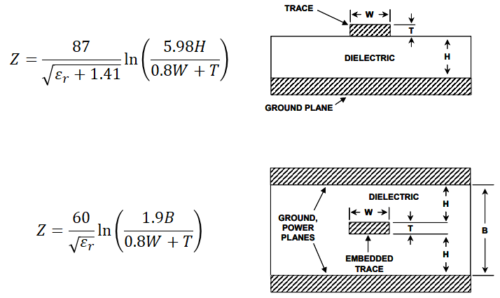
Wadell’s Equations
The IPC-2141 standard is just one source of empirical equations for microstrip and stripline impedance. However, the IPC-2141 formulas for microstrip traces actually produce less accurate results than the equations derived with Wheeler’s method and presented in Brian C. Wadell’s seminal textbook Transmission Line Design Handbook.
The equations in Wadell’s textbook are not necessarily difficult to use; they are analytical equations or special functions with tabulated values, and in principle, they are easy enough that you could create an Excel sheet that powers through the calculations. The difficult part of these equations is the number of parameters that appear in some of the equations. For example, Wadell’s solution for differential pairs includes dozens of parameters that need to be calculated correctly as part of the impedance calculation.
The simplest of Wadell’s solutions is the single-ended microstrip equation without solder mask, which would be applicable in some non-coplanar microwave designs. The impedance equation and effective dielectric constant are:
The trace impedance calculators we developed on Altium Resources are based on Wadell’s equations as derived with Wheeler’s method. While we only address microstrips and striplines (both single-ended and differential), Wadell’s textbook provided derivations for a huge range of transmission lines that may appear in a variety of printed circuit designs.
- Single-ended microstrip calculator
- Single-ended stripline calculator
- Differential microstrip calculator
- Differential stripline calculator
It has become widely accepted that Wheeler’s method (known as conformal mapping) is the most accurate method for calculating analytical solutions for transmission impedance in any geometry. However, these are still lossless results; the lossy results look very different, as discussed in the next section.
Lossy vs. Lossless Impedance
Although I can tell you that lossy and lossless impedance are different, it’s easiest to see why they are different simply by looking at a graph of the lossy impedance.
Lossless impedance actually ignores two factors:
- Dispersion in the dielectric constant (variation with frequency)
- All the loss factors listed above
This means that a trace designed to 50 ohms with a lossless impedance formula will have that value at all frequencies.
Obviously, we know this to contradict reality, and it becomes obvious just by including the dispersion (still no losses). We can also see the expected variation in the impedance if we look at return loss measurements for a transmission line, or if we look at the lossy transmission line impedance calculated with a 3D electromagnetic simulator. A graph of the latter for various roughness values of the copper foil is shown below.

The impedance variation is very clear, and this is why many transmission line designs will require some compensation for the transmission line impedance variation seen in the above graph over large frequency ranges. In other words, if you want to have an approximately 50 ohm line over a broad frequency range, you might want to use 48 ohms as the calculation target in your lossless transmission line impedance calculator; once you add back in the losses, the impedance will vary closer to the 50 ohm target value.
This practice is more common than you may think. I have worked with signal integrity engineers who use lower impedances than the recommended value as the calculation target when selecting an initial design for a transmission line. For example, I recently worked on a project that implemented 25G serial links on the Aurora protocol; the differential pair design was started by using a target impedance of 93 ohms rather than the interface specification of 100 ohms precisely to compensate for the type of variation in the lossy impedance shown above.
Impedance in Altium Designer
Altium Designer includes a semi-lossy impedance calculator inside the Layer Stack Manager.
The impedance calculator is accessed directly through the Layer Stack Manager, where impedance profiles can be defined using the materials and layer geometry in the PCB stackup. To access the calculator:
- Open Design → Layer Stack Manager from the PCB editor.
- Select the Impedance tab in the Layer Stack Manager.
- Add or select an impedance profile for the required routing layer.
- Select the transmission line structure, such as single-ended or differential routing.
- Enter the target impedance and calculate the required trace geometry.
The result from the impedance calculator in Altium Designer is based on an empirical computational electromagnetics model from Simbeor. It is known to be highly accurate as a first estimate for trace impedance that includes losses. It only provides the lossy impedance magnitude at 1 GHz, so some adjustment is needed to take the loss terms and transform them to a higher frequency. However, this is still a very useful place to start as an estimate for the true lossless impedance at higher frequencies.
From my experience, the value given by the calculator should be compensated by 1-1.5 ohms for practical copper roughness values found in commercial materials. In other words, if you want to design a 50 ohm trace at high frequency, you should use a target impedance of 48.5 to 49 ohms in the calculator. I have shown some details and data about this in another article:
The Right Way to Use a Trace Impedance Calculator
If you’re designing impedance-controlled lines with channel bandwidth below 1 GHz, you usually don’t need a full-wave calculation. Get the dielectric data from your PCB materials manufacturer, and use that value in the lossless calculator to get the impedance result. Some of the well-known impedance calculator programs you would download already do this for you.
If you want to use a lossless impedance calculator in your design process for high-frequency lines (well above 1 GHz bandwidth), it is still possible to do this, but you will need to incorporate an electromagnetic simulator into the design process:
- Use compensation to determine a trace width value that is slightly below the desired impedance.
- Create a test trace or apply the trace width directly in your design, and export it to a format that can be used by a simulator.
- Run the simulation to extract the TDR trace and the return loss plot (S11).
- Based on the TDR trace and the return loss, estimate how much the estimated impedance from Step 1 needs to change to get the lossy impedance closer to the target.
- Calculate a new lossless impedance trace width given the required change determined in Step 4, apply the trace width on the desired traces, and re-simulate.
- The return loss will improve, and if it is sufficiently low, then you can lock in the trace width. Otherwise, repeat Steps 2-5.
This is the same iterative process that is generally used for highly accurate impedance-controlled via design, timing adjustments on parallel interfaces (DDR, etc.), and many RF designs.
The other option is to directly convert the true lossless value into a lossy impedance using the method linked above. This relies on having highly accurate dielectric constant data across the desired frequency range. However, it will give a much better picture of the lossy impedance than using a calculator you find on the internet.
Whether you need to build reliable power electronics or advanced digital systems, use Altium’s complete set of PCB design features and world-class CAD tools. Altium provides the world’s premier electronic product development platform, complete with the industry’s best PCB design tools and cross-disciplinary collaboration features for advanced design teams. Contact an expert at Altium today!

About Author
Related Resources
Related Technical Documentation
Table of Contents
Solutions for Every Role and Team
- Discover and evaluate design options earlier
- Develop in one shared workspace
- Scale with control and compliance
- Connect every stage of hardware development
Learn More
Thank you, you are now subscribed to updates.



