


Flex Circuit Specific Terms and Definitions

At a Glance
Learn key flex circuit terms and definitions to navigate flex and rigid-flex PCB design with confidence. Master industry terminology for better designs.


Recently, I had a few discussions with someone who was very new to flex design. I was trying to be helpful and going through several things that are specific to flex and rigid-flex design, which should be considered as you start your first design. He was listening and taking notes and suddenly stopped me and said, "You lost me a few items back; I am not completely sure I understand this terminology." This flashed me back to memories of my early days in the industry, my having also been slightly confused by the terminology. Back then, we didn’t have Google to help us out, either!
This blog is written for those of you who are new to flex and rigid-flex and may be unfamiliar with some of the terms that get volleyed around in conversation.
Elements of a Flex Circuit Design
A flex circuit combines several material layers and design features that work together to deliver both electrical function and mechanical performance. Understanding what each element does before diving into detailed design rules gives you a better foundation for making stackup and layout decisions. The elements described here are covered in greater depth elsewhere in this series; this section is intended as a map of the terrain.
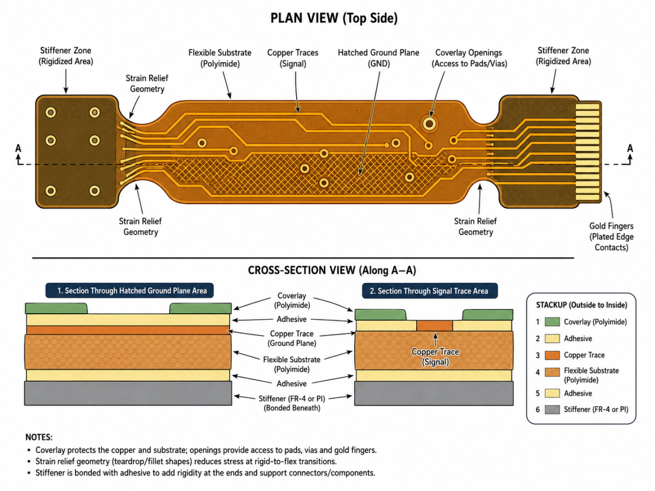
Anchors/Rabbit Ears
Extra copper extended from the copper pad area and encapsulated by the coverlay to help anchor the pad to the substrate. This is recommended for all flex designs and is especially important with single-sided designs that do not have a plated through-hole to help anchor the copper.
Banding
Often used to accommodate a shorter flexible area if there is no room for a service loop. Instead of using the full width of the flex region between areas for each inner layer, the area can be divided into smaller bands of equal width for each inner layer, eliminating buckling and stress in that area.
Bend Radius
This is the ratio of the bending radius measured to the inside of the bend to the overall thickness in that area. Typically, recommendations for non-dynamically flexing designs is 10:1 for single and double-sided construction, and 20:1 for multilayer construction. These can be exceeded but should be evaluated carefully. Dynamically flexing applications should be discussed with your fabricator for a recommended stack up.
Bikini Cut
Coverlay material used to insulate the circuitry on the flexible layers is typically bonded with acrylic adhesives. It is recommended to NOT have acrylic adhesive extend more than .050" into the rigid portion of the design to avoid reliability issues in the plated through-hole areas. Bikini cut refers to cutting back the acrylic adhesive, so it is not extended into the rigid portion of the stack up.
Button Plate
Fabrication process to selectively electroplate copper to vias and onto the pads capturing the vias. The remaining copper traces do not have electrodeposited copper, increasing the flexibility of the circuit.
Cover-Coat
This is typically a photoimageable cover-coat similar to a traditional PCB solder mask but formulated to be flexible. Cover-coats are often used with lower layer count flex, applications without high flexing requirements, and in situations with tight pad features that exceed standard drilled coverlay capabilities.
Coverlay
A layer of insulating material applied to the flexible circuit to insulate the conductor pattern. Coverlay is typically a layer of polyimide with acrylic adhesive. Film-based coverlay is much more flexible than cover-coat materials and is highly recommended for dynamically flexing applications or flex that will have a tight bend radius. It is important to be sure to spec enough adhesive to fully encapsulate the copper conductors.
Fillets
The gradual transition point from pad to the conductor to eliminate stress points. The pad-to-trace interface in a flex design is highly susceptible to cracking or breaking. Filleting is recommended in all flex applications.
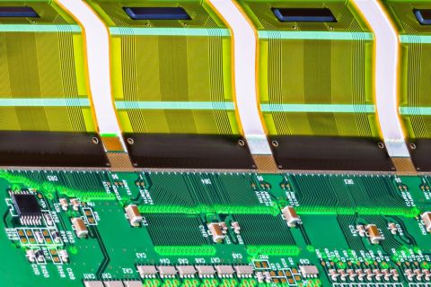
Flex Tails
Typically, it refers to the areas of flex extended out past the rigid portions of the rigid-flex. This may be one flex region or several bands of flex areas that extend in various directions. Rigid-flex is often used to solve packaging issues and connect on multiple planes. Flex tails enable this.
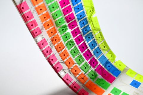
Flexible Circuit
A pattern of conductive traces bonded on a flexible substrate. There are several different substrates available, the most common being polyimide. Different than rigid materials, these laminates will have rolled annealed (RA) copper for improved flexibility.
Gang Open
With drilled overlay, the minimum distance between features is .25 mm. If that space is not available to allow proper registration. Gang opening, opening a block of pads with one single coverlay opening is suggested. If this is not possible, common alternatives include an LPI solder mask or laser cutting of coverlay.
Gold Fingers
Gold fingers are plated edge contacts that let a flex circuit plug into a ZIF connector, card-edge slot, or wiping contact interface. Gold provides a low-resistance, oxidation-resistant contact surface; hard gold is used for high-cycle connections, while ENIG is suitable for low-cycle or static use. The finger pitch, width, length, and insertion-edge chamfer must match the mating connector specification.
Hatched Ground
A hatched ground plane uses copper mesh instead of a solid pour to keep the flex region bendable. It provides a usable ground reference with reduced stiffness, but impedance should be verified by simulation or measurement.
I-Beam Effect
Stacking conductors on adjacent layers directly on top of one another, increasing the stiffness of the circuit in the bend or fold areas. Staggered conductors are recommended, if possible, to retain the maximum flexibility of the circuit.
Pouch
This is a protective barrier material often used in rigid-flex fabrication. Often, this is a coverlay material used to protect exposed flexible materials during processing and is removed from the flexible portion of the board before shipment.
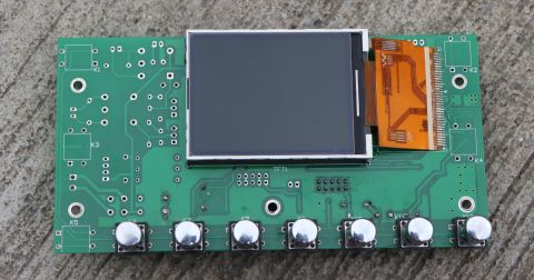
Rigid-Flex
This is a hybrid construction, using flex materials in areas that need to bend or flex and rigid materials in areas with dense component areas, surface mount components on both sides of the PCB, and applications with higher layer count, dense routing areas. Most common rigid materials can be incorporated into a rigid-flex construction.
Squeeze Out
As the coverlay is pressed and cured, the acrylic adhesive will "squeeze out" onto the pad area. Attention should be given to the size of the coverlay opening and pad size to factor this into annular ring calculations.
Stiffener
Stiffeners are rigid materials (e.g., FR4, polyimide) bonded to localized areas of a flex circuit, typically behind connectors, to provide mechanical support against stress. They must be specified in fabrication drawings by material, thickness, and bonding method.
Strain Relief
Strain relief prevents fatigue cracking by reducing mechanical stress at transition points between flexible and rigid sections. It is implemented via geometry changes, supplemental adhesive/coverlay, or mechanical supports, tailored to static or dynamic applications.
Conclusion
I hope this helps explain some of the common terminology with flex and rigid-flex materials and design. Talk to an Altium expert today to learn more or continue reading about why Altium Designer® is the best design solution for rigid-flex PCB Design.
About Author
Related Resources
Related Technical Documentation
Table of Contents
Design to Release, Without the Friction
- Keep reviews tied to the right version
- Reduce handoff confusion and rework
- Spot sourcing and release risk earlier
- Work solo, share when needed
Get Started
Thank you, you are now subscribed to updates.