







Getting Started With a PDN Analyzer For DC Power Integrity

At a Glance
Learn about PDN analyzer simulators for PCBs. These systems provide simulations for power electronics, high-speed systems, and many other applications.


Copper has low resistance, so we generally don’t need to worry about the voltage drop across copper features in a PCB, right?
Just some simple, back-of-the-envelope calculations with practical copper features reveal that this may not always be the case. At low current, voltage drop in copper features will always be small, but voltage drop becomes significant as current increases due to IR drop. The voltage drop across copper conductors can become so large that it creates excessive heat, or the voltage drop across the rail is so large that components will not turn on, or both.
A PDN analyzer is used to diagnose these problems in both types of systems, which may be at the extreme ends of DC versus high-speed digital design. So in this article, we’ll examine its role in DC power integrity and how you can get maximum value from PDN analyzer results in your PCB.
What Is a PDN Analyzer?
A PDN analyzer for DC power analysis calculates the voltage lost as current flows through PCB copper. The analysis includes the resistance of power and return paths, allowing the designer to determine whether sufficient voltage reaches each load. This becomes useful when narrow copper connections, long supply paths, or high load currents consume a substantial portion of the available voltage margin.
Power Analyzer by Keysight performs this analysis within Altium Designer using the PCB’s physical copper geometry and connectivity. The designer defines the electrical conditions applied to that geometry, including sources, loads, and series components. A complete power network includes the return connections because resistance in the ground path also contributes to the voltage difference seen by a load.
The simulation combines information extracted from the design with electrical inputs and acceptance limits supplied by the designer:
Analyzer Input | Information Required |
PCB Geometry | Copper shapes, conductor thicknesses, via dimensions, and plating thickness |
Sources and Loads | Supply voltages, load currents, and associated power and reference nets |
Series Components | Resistance or voltage drop through components such as fuses and resistors |
Material Properties | Copper properties and working temperature used to determine resistance |
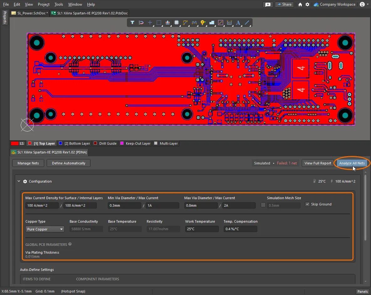
The results show voltage distribution and current density across the modeled copper, together with current through vias. Heatmaps relate these values to specific layout features, while probes provide numerical results at selected locations. A narrow copper bridge may produce a concentrated voltage gradient, and a group of vias may carry current unevenly despite appearing adequately sized in the layout.
These results support decisions about copper width, layer allocation, and via placement. The useful verification is whether the revised layout delivers the required load voltage within the specified current limits. Regions with concentrated current also warrant closer investigation for resistive heating.
Two Common Applications: DC Power Electronics and Digital Systems
PDN Analysis in DC Power Electronics
In a DC power system, the goal is to deliver stable power with a defined DC voltage, often at high current. The PDN in a DC power system drops voltage as current moves between regulation stages and, ultimately, to the system output, where it is accessible to a user. A PDN analyzer takes the current inputs and target voltages from the user and calculates the DC resistance across the copper nets in the PCB layout, and the voltage across the net is displayed to the user.
The standard visualization for a PDN analyzer output when determining voltage drop is a heatmap. The heatmap uses a color scale to show the voltage at each point in a copper net. A simple example in an Altium reference design is shown below.

Additional views are available for current density, and even for temperature in some simulators. The combination of current density and voltage indicates locations where high power dissipation occurs, potentially leading to hotspot formation. If hotspots form and result in repeated thermal cycling, this may result in thermomechanical failure at that location on the board, particularly when vias are nearby.
Voltage drops are quite important when the output of a power system is connected to a measurement interface or a downstream regulator with low headroom. If not accounted for, the downstream circuit may not measure the voltage accurately or turn on. High-power, regulated power electronics require accurate voltage values, and a PDN analyzer can predict these problems during the design phase.
High-Speed Digital PCB Designs
In high-speed digital systems, large processors and many I/Os switching with fast edges create rapid changes in supply current. These transients interact with the PDN’s inductance and capacitance, producing voltage fluctuations at component power pins. AC and transient simulations typically calculate:
- PDN impedance versus frequency
- Resonance and antiresonance frequencies
- Supply voltage ripple under the specified current excitation
- Dynamic voltage droop/overshoot and ringing during load transitions
In large processors with very high currents, DC simulations are also needed to measure the voltage drop along copper rails. Large processors and FPGAs with high pin counts are operating with low core voltages, reaching down to 1.0 V or less. These low core voltages are used because the processors will demand very high current, and at high current, the resistance of the PDN can drop some voltage before power reaches the power pins of the processor.
With today’s large, cutting-edge processors running at kA levels, we now demand DC PDN resistance below 1 mΩ in order to ensure minimal voltage drop. For example, sometimes we have a DC rail on a PDN targeting a 0.8 V core voltage at 800 A; a DC resistance on the power rail of 200 µΩ would result in a voltage drop of:
(0.2 mΩ) × (800 A) = 160 mV
This is a large enough voltage drop to drop the voltage below the minimum threshold to turn on the processor.
Typical Fixes for High DC Resistance
The fixes that can be implemented in digital systems are similar to the preferred approaches in DC power electronics. Generally, designers will take one of these approaches:
- Use heavier copper on the power rail layers
- Parallel the power rails onto multiple layers
- A combination of 1 and 2
In DC power electronics with low component count and low density, option one is typically the best approach, although this can make assembly challenging for some vendors. In high-speed digital systems, option two is the only option, and this may require reducing copper weight on the power rails rather than increasing it.
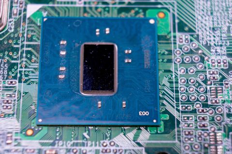
It is easy to see why this is the case when looking at a through-hole via field below a processor in a BGA package. Consider the image below; if we were to increase the copper weight on this layer, it would demand increasing the clearances between the copper features, and overall, it may increase the DC resistance. Instead, we would want to decrease the allowed clearance, which requires decreasing copper weight, and we could also decrease the via size and pad size if aspect ratio limits and annular ring limits allow.
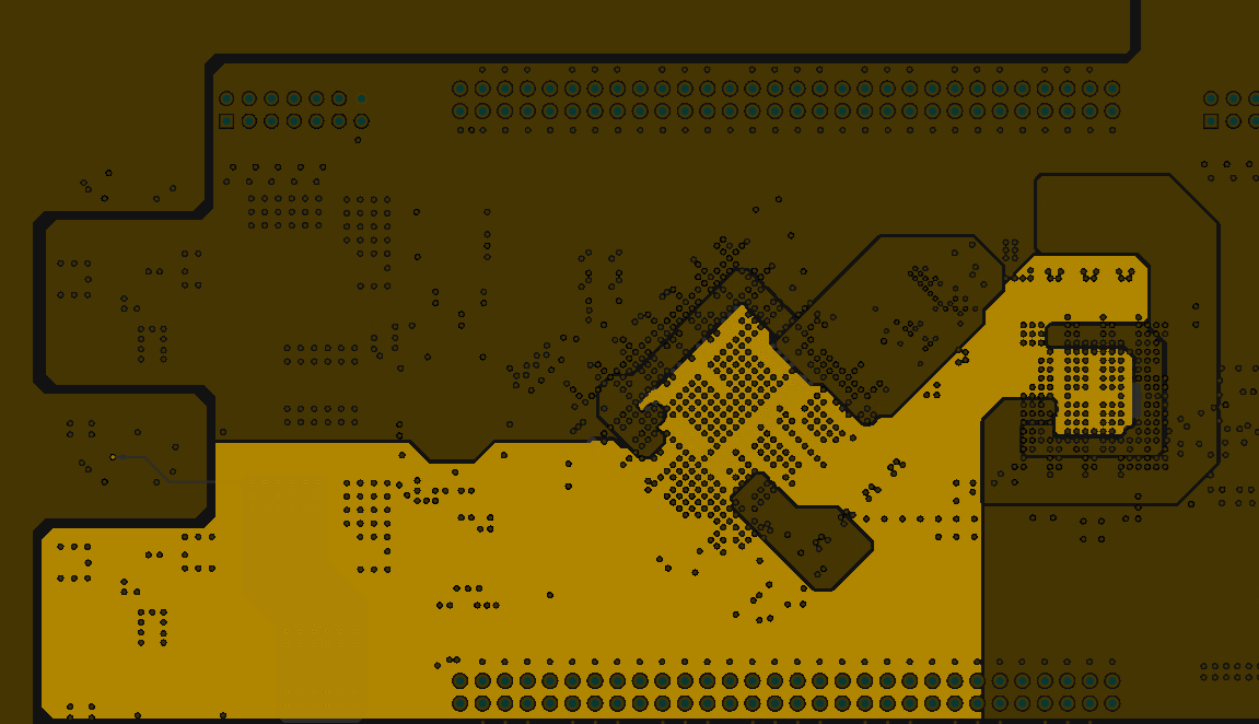
These PCB layout updates are very easy to implement and can be quickly verified in a PDN analyzer. These simulations are steady-state and can run very quickly, often in a matter of seconds on a basic laptop.
What Are the Best PDN Analyzer Solutions?
Altium users previously performed DC power integrity analysis with the CST-powered PDN Analyzer extension. Altium now directs users to Power Analyzer by Keysight for its latest DC analysis functionality. The extension uses the current PCB project, allowing designers to investigate power delivery and evaluate layout changes within the same environment used to create the board.
The analysis supports hierarchical power networks containing sources, loads, voltage regulators, and series components. Its results provide several ways to investigate a supply path:
- Voltage-drop heatmaps showing how the supply voltage changes across the copper
- Current-density heatmaps identifying narrow connections and concentrated current paths
- Via-current results showing where layer transitions exceed configured limits
These views connect an electrical problem to the physical feature responsible for it. Measurement probes provide values at selected locations, and reports document the calculated results and violations. After a copper or via change, another analysis shows whether the revised geometry provides sufficient improvement. Automatic power-net identification can also reduce setup work, although the resulting network still requires review.
Result accuracy depends on the copper model and the electrical conditions applied to it. Copper thickness, via plating, temperature, source voltage, and load current all affect the calculated drop. The schematic and PCB must remain synchronized so the analysis represents the intended design. These predictions support layout decisions, while measurements on the assembled board verify power delivery under actual loading conditions. Hardware verification also helps establish whether the selected simulation conditions adequately represent the product’s current demand.
Whether you need to build reliable power electronics or advanced digital systems, use Altium’s complete set of PCB design features and world-class CAD tools. Altium provides the world’s premier electronic product development platform, complete with the industry’s best PCB design tools and cross-disciplinary collaboration features for advanced design teams. Contact an expert at Altium today!
Frequently Asked Questions
What Does a PDN Analyzer Calculate in a PCB?
A DC PDN analyzer calculates voltage drop and current distribution through the PCB’s power and return conductors. It uses copper geometry, material properties, and defined electrical loads to identify excessive voltage loss, concentrated current density, and overloaded vias.
What Inputs Are Required for DC PDN Analysis?
DC PDN analysis requires source voltages, load currents, power and reference nets, and the PCB’s copper geometry. Copper thickness, via plating, working temperature, and series-component resistance affect the results. Allowable voltage drop and current limits establish the acceptance criteria.
What Is the Difference Between DC and AC PDN Analysis?
DC PDN analysis evaluates resistive voltage drop under steady loading. AC PDN analysis calculates impedance versus frequency and identifies resonances. Transient analysis predicts voltage droop, overshoot, and ringing during changes in load current, helping designers evaluate decoupling and supply-voltage stability.
Why Do High-Current Processors Need DC PDN Analysis?
High-current processors combine substantial current demand with low supply voltages, leaving limited margin for resistive voltage loss. Even a small resistance between the regulator and processor can consume a significant portion of the permitted voltage tolerance, requiring analysis of the complete supply and return paths.
Does DC PDN Analysis Include the Ground Return Path?
A complete DC PDN analysis includes both the supply conductor and its return path. Resistance in either path reduces the voltage available across the load’s power and ground pins. Evaluating both paths helps identify losses that would be missed by examining the supply rail alone.

About Author
Related Resources
Related Technical Documentation
Table of Contents
Solutions for Every Role and Team
- Discover and evaluate design options earlier
- Develop in one shared workspace
- Scale with control and compliance
- Connect every stage of hardware development
Learn More
Thank you, you are now subscribed to updates.