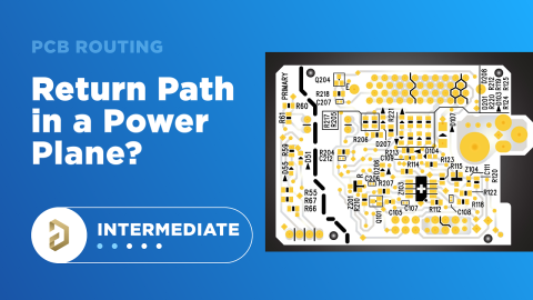


Power planes (sometimes called a power layer) and ground planes are important for more than just distribution of supplying power. When defining reference planes, both with impedance controlled routing and in managing return paths, your stackup might force return currents to pass into a PCB power plane before being coupled back to a ground layer. Even though you define a GND reference layer as a the basis for your impedance-controlled trace width
Learn all about proper use of a PCB ground plane and grounded copper pour in your design. You’ll ensure signal integrity and low EMI with correct PCB ground plane placement.
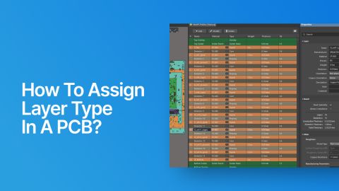
How to assign layer types in a PCB? Expert Phil Salmony shares with us some of his favorite multilayer stackups, complete with guidelines.
Stack-up choices shape PCB performance, reliability, and manufacturability, especially in flex and UHDI. Learn how to design with materials in mind.
Avoid warpage, impedance issues, and delays. Learn how smart PCB stack-up design ensures performance, reliability, and smooth fabrication.
PCBs with mechanically drilled blind and buried vias use sub-laminations which differ from sequential lamination significantly.
Your high voltage PCB design will need a board material that’s specifically designed to tolerate high voltages, as well as potential for overvoltage and high temperature.
The PCB is designed and formed as a stack of layers. In the early days of printed circuit board (PCB) manufacturing, the board was simply an insulating core layer clad with a thin layer of copper on one or both sides. Connections are formed in the copper layer(s) as conductive traces by etching away (removing) unwanted copper. Fast forward to today, where almost all PCB designs have multiple…
The Role of the Via Vias are used to create the vertical, or layer-to-layer connections in a printed circuit board. In the early days of board fabrication, all of the vias passed all the way through the board, from one side to the other. These thru-hole vias are drilled after the layers are fabricated and the routing etched. The conductive via barrels are formed in the drilled holes using an…
Solutions for Every Role and Team
Discover and evaluate design options earlier
Develop in one shared workspace
Scale with control and compliance
Connect every stage of hardware development
Learn More