


Slaying the PCB 90⁰ Right-Angles Bend Dragon

At a Glance
One of the areas where misinformation continues to abound focuses on 90° angle bends in PCB traces. Get the facts of the matter here from expert Kella Knack.


As anyone designing PCBs knows, there are a lot of “Rules-of-Thumb” and myths that have populated the industry. One of the areas where misinformation continues to abound focuses on 90° angle bends in PCB traces. A pretty good job has been done to address some of the most outlandish aspects of the bad data such as avoiding right-angle bends because electrons would go flying off the corners and not using them because the copper in the corners can flake off (although it should be noted that a recent search on the Internet yielded yet another iteration of the copper-flaking myth).
There are two areas where correcting the right-angle bend myth continue to remain “fuzzy”: Signal Integrity (SI) and Electromagnetic Magnetic Interference (EMI) Electromagnetic Interference (EMI). This blog will focus on these two areas. Further on, empirical information will be presented that proves why the following assumptions are erroneous.
Signal Integrity
First Assumption
When you are designing high-power PCB transmission lines at RF frequencies, you are involved with circuits that use trace widths of 100 mils and, as a result, you need to worry about 90° angles. The assumption is that the extra width in the corner is capacitance that can cause an impedance variation which can lead to reflections, signal distortions and noise along the trace. This is simply not true. Rather, this is a concept borrowed from RF and microwave design guides used in the development of high-power RF circuits. In a megawatt transmitter you have thousands of volts. If you have right-angle bends, there is corona discharge caused by sharp points. This does not occur in low-power PCB implementations such as logic circuits.
Second Assumption
It is safe to use right-angle tracks in your design as long as you are not working on ultra-high frequency microwave designs. The truth is that frequency is not an issue of concern. If you examine the impedance between a 45° degree track and a right-angle bend, you cannot tell the difference between the two. The signal does not either. Evidence presented below shows this is not so.
EMI
The Assumption
With right-angle bends, electronic fields become concentrated at the corners. This results in destructive electromagnetic radiation coming from those corners that manifests itself as EMI. Evidence presented below shows this is not so.
The Proof Is in the Test Results
TDR Results
To validate the claims made regarding the impact of right-angle bends, a 16-layer test PCB containing more than one hundred different test structures was built to address the long-held impedance and EMI claims. That board is depicted in Figure 1.
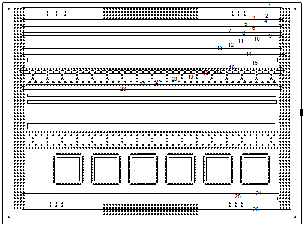
Figure 1. Layer Artwork of Test PCB
Trace 15 has a right-angle bend near each end. Traces 24 and 25 have right-angle bends in them in their lower right-hand corners. To test these three traces, a Time Domain Reflectometer (TDR) with a rising edge of 125 picoseconds was used to determine if these right-angle bends cause any change in impedance. If there is any meaningful degradation from these bends, there should be a detectable change in impedance that is visible on the TDR trace. A lowering of impedance would be depicted as a reflection that is “negative” going. A rise in impedance would be depicted as a reflection that is “positive” going.
Figure 2 contains the three TDR plots for the three test traces. The first dip in impedance is where the test cable makes contact with one end of the trace at a via. The second dip in impedance is the test via at the opposite end of the trace. The flat portion between these two dips is the trace under test.
Figure 2. TDR Records of Three Traces with Right Angle Bends
It can be seen from these tested traces that the right-angle bends caused no detectable change in impedance even with an edge of 125 picoseconds. In a related test PCB, done by a group of engineers and tested at the University of Missouri, Rolla, a right-angle bend was tested with an 18 picosecond edge and the same results were achieved. In that same test, as reported in Printed Circuit Design Magazine, titled “90° Corners, The Final Turn,” by Douglas Brooks, (January 1998), right-angle and acute-angle bends were tested for reflections and as potential sources of EMI with negative results.
If one closely examines a right-angle bend, it can be determined that for a very short distance, the effective width of the trace is wider. However, for such a short distance, there is no detectable change in either Co (parasitic capacitance) or Lo (parasitic inductance). These two variables have to be affected in order for a reflection to occur.
This particular myth arose as a result of one particular figure (Figure 7-17) appearing on one particular page (page 138) of the Motorola MECL Systems Handbook that was published in 1971, and later reprinted in 1980 and 1989. This figure shows two traces, side-by-side, one with two right-angle bends and the other with those bends rounded. Below that picture are two oscilloscope traces. The trace for the right-angle bend example has two small dips in the middle of it while the trace for the rounded corners has none. This suggests that right angle-bends cause a problem.
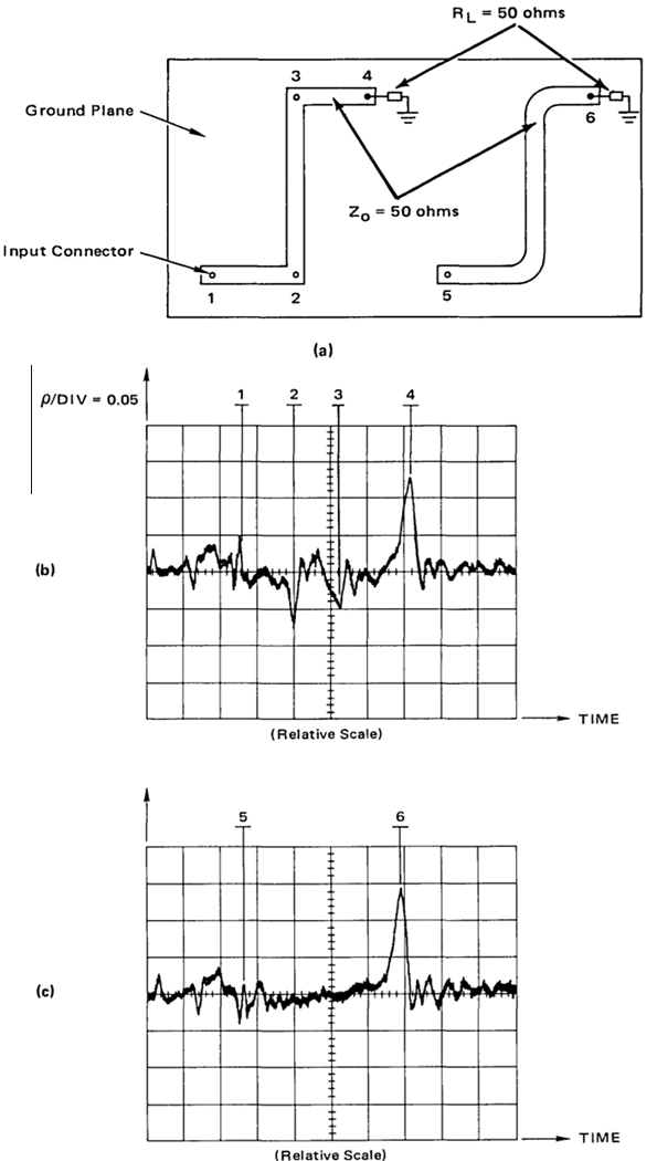
Figure 7-17 from Motorola MECL Systems Handbook.
Unfortunately, the description from the MECL book does not contain an important piece of information: the rise time of the TDR signal. As was mentioned above, even a relatively fast TDR pulse of 125 picoseconds can fail to detect a right-angle bend, and thus we would say that digital signals with edge rate of 125 picoseconds or longer will be unaffected by 90-degree bends. We need this in order to understand how the approximate frequency range where the TDR signal can detect an impedance discontinuity, and this will tell us whether such a reflection actually matters for a particular digital interface.
S-parameter Results
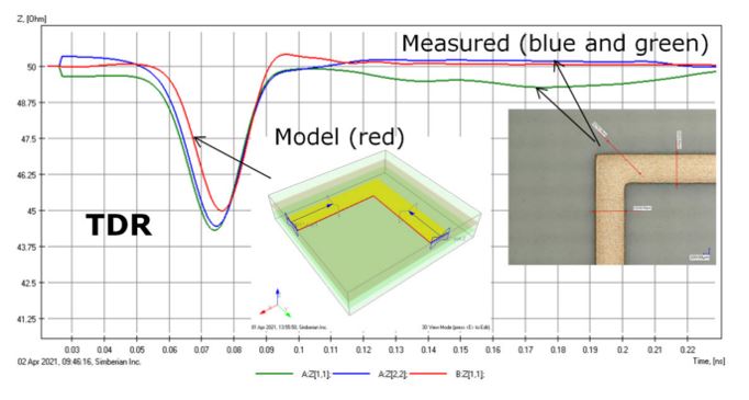
We can get a better sense of the impact of 90-degree bends on signal integrity if we look at some simulation data provided by Zach Peterson. He modeled three routing configurations in Simbeor using a standard stackup with microstrip routing over a ground plane, targeting 50-ohm single-ended and 100-ohm differential impedances. The three configurations compared a right-angle bend, two 45-degree turns, and an arc turn.
We can get a better sense of the impact of 90-degree bends on signal integrity if we look at some simulation data provided by Zach Peterson. He modeled three routing configurations in Simbeor using a standard stackup with microstrip routing over a ground plane, targeting 50-ohm single-ended and 100-ohm differential impedances. The three configurations compared a right-angle bend, two 45-degree turns, and an arc turn.
For single-ended transmission lines, the S-parameter results from both the Fast SI and full 3D simulation algorithms show no meaningful difference in return loss across the three configurations up to well beyond practical operating frequencies.
- The TDR data does show a slight impedance deviation at the 90-degree bend, but the magnitude is approximately 0.5% larger than the other two configurations, which is too small to appear as a distinguishable feature in the S11 plot.
- Differences in total insertion loss between the three traces follow trace length, not bend geometry, with the 90-degree route being the longest and therefore showing the highest loss.
- Differential transmission are well-behaved up to approximately 80 GHz, where the right-angle pair shows about a 3-ohm impedance deviation at the bend, equating to a 3% difference from the 100-ohm target.
- Above 80 GHz, return loss diverges slightly, and at 115 GHz, the right-angle differential pair exhibits a localized dip in insertion loss consistent with an anti-resonance
Another resource showing simulation data from Eric Bogatin shows that the reflections could be observable under certain situations. In his Signal Integrity Journal article, titled "Should You Worry About 90 Degree Bends in Circuit Board Traces?" Eric Bogatin shows data revealing that a 5-mil trace width would only experience 8.5 fF of capacitance and that this would not produce any noticeable impact on signal integrity until we are looking at frequencies well over 70 GHz.
However, a much wider trace will have a much larger excess capacitance. A right-angle turn in a 20-mil wide trace does not create a 10% impedance deviation until 60 GHz, and even an egregiously large 120-mil wide trace with a right-angle turn still does not show 10% impedance deviation below 10 GHz.

Graph from Bogatin's Signal Integrity Journal article showing (Top) impedance deviation from a TDR plot and (Bottom) return loss for various trace widths with right-angle bends.
The article also shows that the reflections can be measured from a TDR trace, similar to the MECL results shown above. On this point, Dr. Bogatin states clearly:
TDR rise time simulated and measured was about 20 psec. It shows an impedance dip of about 5 Ohms for this rise time…A shorter rise time would result in a larger impedance dip. A longer rise time in the TDR response would result in a smaller impedance dip for the same corner feature.
This is because of the input impedance seen at the corner bend, which is a function of the length of the discontinuity along the propagation direction. This can be re-cast in terms of rise time as is typically done when talking about critical lengths. This nicely explains why some reflection measurements from 90-degree bends may be quite difficult to see in measured data: they require a very fast input pulse to create a sufficiently large reflection. In fact, most commercially available TDRs for PCB trace testing have longer rise times, on the order of approximately 100 ps or more.
The Manufacturability Consideration
In addition to the foregoing, there is one final argument to consider regarding right-angle bends and that deals with PCB manufacturability. The assumption was that right-angle or sharp angle bends used to present a realistic threat to manufacturability. Sharp corners would create acid traps and these acids would corrode the copper in the sharp corners. The realty is if there were acid trapped anywhere on a copper layer, it would cause leakage problems later in the process so PCB fabricators made sure the rinse operations did not leave any acids or other chemicals anywhere on a PCB.
Further, in the early days of PCB fabrication, there was a problem with the process used to image PCB copper layers for etching. The first process used was silk screening not unlike the process used to put an image on a T-shirt. When there were right angles or acute angles in the copper, the ink from the silk screen would often bleed into the tight corner leaving an unattractive looking feature when etching was completed. This only caused cosmetic problems not electrical ones. Inspectors would often reject PCBs with this type of blemish because they did not look right. The simplest way to avoid these rejects was to prevent this kind of junction between two pieces of copper. It’s quite likely that this rule morphed into the acid trap rule that is still sometimes being passed around the industry.
It was also assumed that right-angle corners weren’t as sturdy as 45° ones and could be peeled off easily (note the statement at the beginning of the article regarding copper flaking). The reality is that right-angle bends are no less robust from a structural standpoint than rounded corners.
The key takeaway here is avoiding 90 degree angle bends in PCB traces is not relevant.You have only to look at other elements within a PCB design to see that this is true. Traces turning and going up a via have right-angle bends. Also, if you lift the lid off an IC you will see that the tracks have right-angle bends. Most importantly, if you waste a nanosecond in making right-angle bends on your PCB traces go away, you are wasting your company’s money and making your designs far more complicated than they need be.
Designing with Confidence
Many long‑standing PCB "rules" persist not because they are correct, but because they were never re‑examined in the context of modern materials, fabrication, and measurement data. The discussion around right‑angle bends is a clear example: assumptions carried forward without validation can lead to unnecessary design complexity and wasted engineering time.
To conclude:
- Long TDR pulses (125 picoseconds) fail to detect right-angle bends with practical trace widths (~5-10 mil), so digital signals are likely to be unaffected as well.
- Bogatin's results (citing Yuriy Shlepnev) show that 20 picosecond TDR pulses can detect ~10% impedance deviations in small traces; this corresponds to channel bandwidths above 70 GHz in practical trace widths.
- The results will be different for single-ended traces vs. differential pairs.
Altium Develop helps engineers make decisions based on real design intent and validated constraints. By keeping schematic, layout, and supporting engineering context connected in one place, it becomes easier to challenge assumptions, validate design choices, and move from design to review to release with clarity and confidence.
Instead of over‑engineering layouts to avoid problems that don’t exist, engineers can focus on what truly matters: signal integrity, manufacturability, and performance guided by data.
References
Ritchey, Lee W. and Zasio, John J., “Right The First Time, A Practical Handbook on High-Speed PCB and System Design, Volume 1.”
Brooks, Douglas. “90 Degree Corners, The Final Turn,” Printed Circuit Design, January 1998.
About Author
Related Resources
Table of Contents
Design to Release, Without the Friction
- Keep reviews tied to the right version
- Reduce handoff confusion and rework
- Spot sourcing and release risk earlier
- Work solo, share when needed
Get Started
Thank you, you are now subscribed to updates.

