









What is Carry Propagation Delay in High Speed Data Processing?


Propagation delay is normally discussed as a property of individual logic gates, but it becomes more significant when several logic functions operate in sequence. Each gate, LUT, register, comparator, or other logic block requires a finite amount of time to respond to a change at its input, and these delays accumulate in cascaded logic blocks.
Carry propagation is a specific example of this behavior. In arithmetic logic, one stage can generate a carry that becomes an input to the next stage. The final output cannot settle until that carry has propagated through every dependent stage. The same timing principle applies to many other fast logic-processing functions implemented with discrete gates, programmable logic, FPGAs, or mixed-signal devices such as GreenPAK.
Propagation Delay Through Programmable Logic
A ripple-carry adder is a good example of a circuit that provides a simple way to see the effects of cumulative logic delay. Each bit position includes logic that calculates a sum and produces a carry output that is passed into the next bit position. Then another calculation is performed and the process repeats until all bits have been processed.
If the least significant bit generates a carry, that state may need to propagate through several stages before the most significant output reaches its final value. For a simplified chain containing N identical stages, the total delay can be approximated as:
Total delay = N*(prop. delay)
In other words, the total time required for the output to propagate after the input is received in the circuit is N*(prop. delay).
The exact implementation is more complicated because different logic elements in a cascade of logical steps have different rising and falling delays, but the idea holds true in cascaded logic processing: each new cascaded stage adds its delay to the previous stage. The important design point is that the longest dependent chain determines how quickly the complete logic function can produce a valid output. This is one reason why we may perform processing at a lower clock rate with data passage controlled on rising or falling edges, because it allows time for the delays to occur and settle during a clock cycle.
The same problem appears in programmable logic even when no arithmetic operation is involved. Consider a signal that passes through several LUTs before reaching an output:
Input → LUT1 → LUT2 → LUT3 → Output
A transition applied at the input does not appear immediately at the output. LUT1 must respond first, followed by LUT2 and LUT3. The output therefore becomes valid only after the transition has propagated through the entire logic chain.
Now when we have a situation with multiple cascaded LUT operations occuring in parallel and feeding into the same receiver circuit, the propagation delays between the two legs significant. Two signals might begin changing at approximately the same time but pass through different numbers of logic elements before reaching a common destination, so their arrival times can differ even when they originated from the same event.
Carry and Logic Propagation Delay in GreenPAK
GreenPAK devices allow multiple programmable functions to be connected internally, including LUTs, counters, flip-flops, delays, analog comparators, oscillators, and other configurable macrocells. These blocks can be combined into relatively complex logic without adding a microcontroller or external programmable logic device. However, the same cumulative timing behavior still applies, especially when processing multiple signals in parallel with different logical paths.
A common example implemented in GreenPAK devices is shown below, where two parallel processing paths applied to some input signal (note each LUT can have additional inputs from other sources). The LUT stages are compared with a XOR gate and the output is passed elsewhere in the system. The logic flow diagram and timing diagram below show what happens when the path along Path A is not appropriately buffered: hte XOR gate gets triggered before Path B has finished processing data through the 3 LUTs.
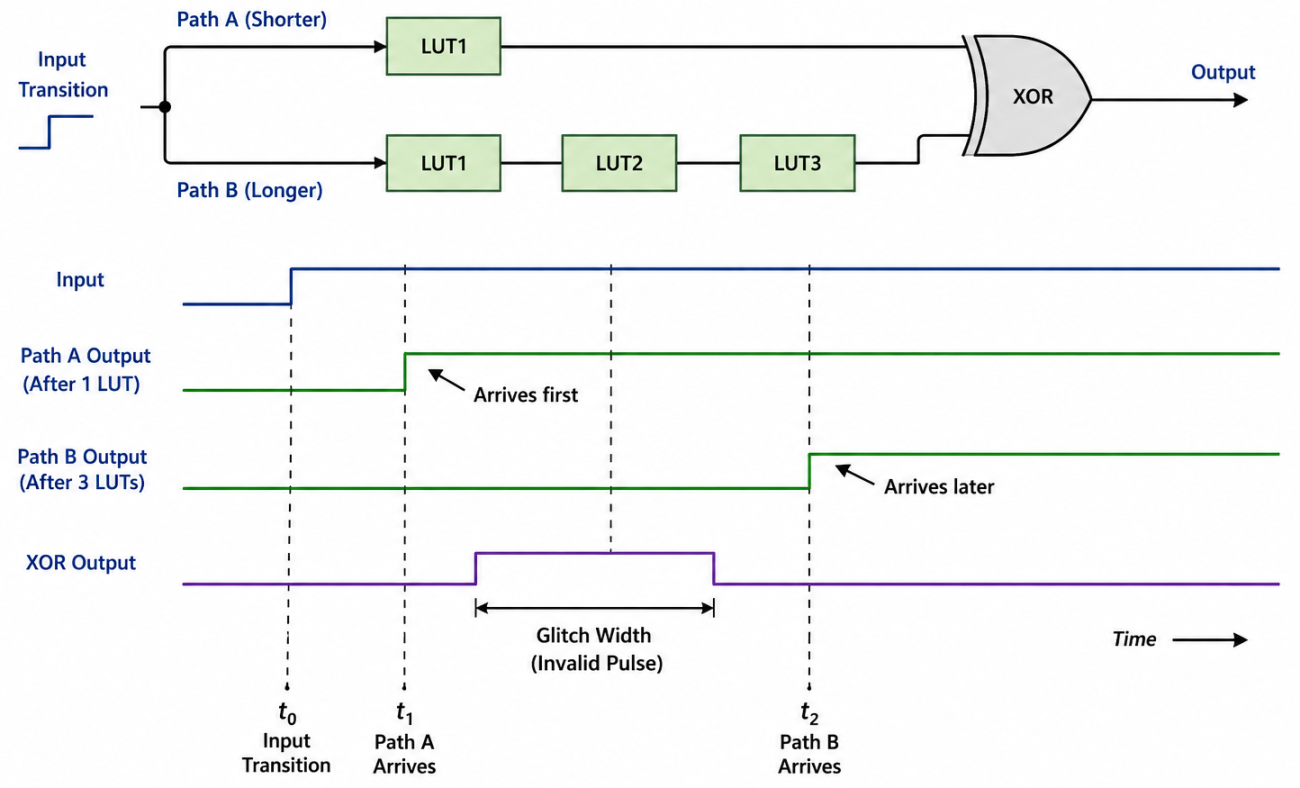
Example logic process with LUTs and a control input.
To fix this issue, either clock needs to be sufficiently slow, or buffering is needed prior to the XOR gate to ensure the total propagation delays in each path are effectively equal. The same problem can occur with AND, OR, multiplexer, and state-control logic. It is most relevant when the output controls another asynchronous function that can react to a very short pulse.
While specific solutions depend on the exact logical processing steps and problem in question, there are some general options to explore:
- Reduce unnecessary combinational logic depth.
- Keep parallel paths reasonably balanced when they reconverge.
- Use registers or other sequential elements when a deterministic timing boundary is required.
- Filter or intentionally delay signals when short transient states cannot be tolerated.
We can identify the timing mismatch by examining the system in a timing simulation. For GreenPAK devices, this would be done in the Go Configure software, which can provide highly accurate timing simulations on target GreenPAK devices.
Checking Timing in Go Configure
The Go Configure software for GreenPAK devices provides a practical way to examine this behavior before committing a GreenPAK design to hardware. Once the design is created, integrated simulation can be used to examine timing across the design with multiple probes placed at strategic points in the design schematic. This includes simulation of parallel processing branches in a design, which is where digital systems become particularly prone to failure due to timing mismatches.

The developer tools in Renesas GreenPAK give designers the ability to develop fully custom digital, analog, or mixed signal ICs that provide a dedicated level shifting function, or level shifting as a built-in feature. These programmable mixed-signal processors allow consolidation of additional logic functions instantiated directly in silicon, allowing for smaller, more efficient systems.
To learn more, take a look at the GreenPAK components and reference examples.
Whether you need to build reliable power electronics or advanced digital systems, use the complete set of PCB design features and world-class CAD tools offered by Altium to implement your GreenPAK solutions. Altium provides the world’s premier electronic product development platform, complete with the industry’s best PCB design tools and cross-disciplinary collaboration features for advanced design teams. Contact an expert at Altium today!
Related Resources
Related Technical Documentation
Thank you, you are now subscribed to updates.

