








Why PCB Designers Can Benefit From a Free Gerber File Editor

At a Glance
Looking for a Gerber file maker online? For the best success when manufacturing your PCB design, you need the latest Gerber X2 file formats in the free Gerber editor in your PCB design tools.


The entire point of using PCB design software is to generate a manufactured file package, the most common being Gerber files. Once these are generated, they will be reviewed with your manufacturer's CAM department, and a CAM engineer may suggest edits to the PCB layout or implement some changes on their own. When asked to make an update to the design, most designers will not update the Gerber files directly, but they will instead update their PCB layout and generate a new manufacturing file package.
However, in some cases, designers need to make edits to Gerber files directly. For example, in legacy designs where the original CAD files are inaccessible, but a basic trace routing update is needed. CAM software is needed to make these updates, and the occasional CAM software user will probably look for a free Gerber file editor. But when your PCB design software includes a built-in Gerber editor, you won't need to search for a third-party program.
What's There to Edit in a Gerber File?
Gerber files are photoplot files. They were originally designed to drive a photoplotter that would expose film using light from a lamp or laser, and that film would then be used to create the tooling needed to fabricate each layer of a printed circuit board. Every copper layer, solder mask layer, silkscreen layer, and paste mask layer in a PCB is represented as a separate Gerber file containing a 2D image encoded in an open ASCII vector format. The fabricator uses these images to create stencils, etch masks, and other fixtures required during board production.
- The data in a Gerber file is human-readable ASCII text, and it encodes the following elements:
- Configuration parameters that define units, coordinate format, and other global settings
- Aperture definitions that describe the shapes and sizes of pads, traces, and other features
- XY coordinate locations that specify where draw and flash commands are executed
- Draw and flash command codes that tell the photoplotter whether to expose a shape at a fixed location (flash) or trace a path between coordinates (draw)
When a Gerber viewer or CAM tool reads these commands, it reconstructs the image of each PCB layer. Round pads on through-hole pins appear as flash commands at specific coordinates, while traces appear as draw commands following a series of vertex locations. Stacking all layers together in a viewer recreates the full board image as you would see it in your ECAD tool.
The two primary Gerber formats in use today are RS-274-X and Gerber X2. RS-274-X combines all four data elements into a single file per layer, with the layer function identified by the file extension. Gerber X2 builds on this by embedding additional metadata directly in the file, including layer function identifiers, pad type definitions, and locations of impedance-controlled traces. A newer Gerber X3 format extends this further, bringing the format closer to intelligent data formats like ODB++ or IPC-2581. Regardless of version, the underlying structure remains a photoplot instruction set that defines geometry on a per-layer basis.
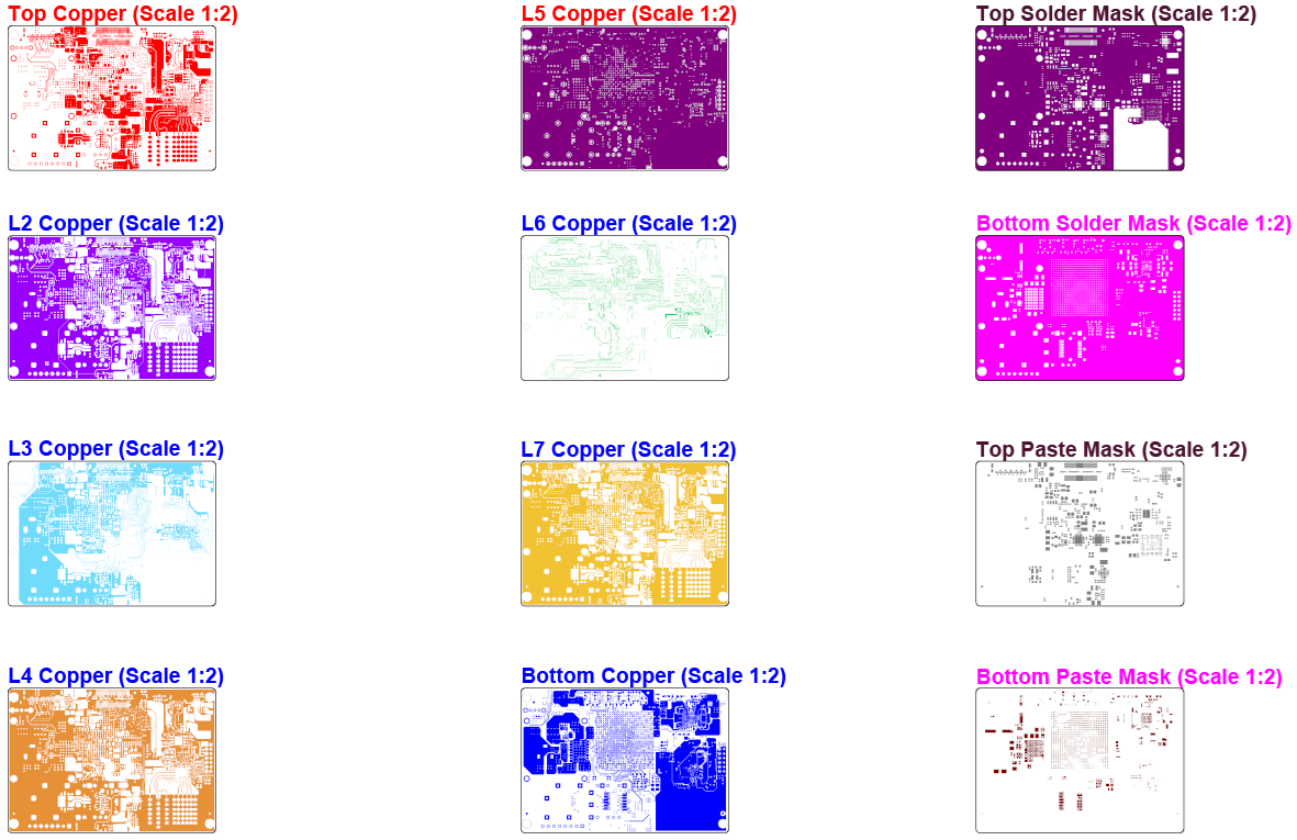
The range of edits you can make in a Gerber file depends entirely on the CAM software you are using. Because Gerber data encodes geometry as draw and flash commands with associated aperture definitions, any object visible in a Gerber layer is theoretically modifiable at the data level. A sufficiently capable editor can reposition pads, adjust trace segments, modify aperture sizes, add or remove features, and alter layer-level attributes. Some manufacturers routinely make small corrections to Gerber data by hand in a text editor and then verify their changes in a viewer.
Most Gerber viewers, however, provide no editing functionality at all. They simply allow visualization of individual layers or a composite stack, which is useful for design review but insufficient when actual modifications are required. Free online Gerber viewers fall squarely into this category. To perform real edits, you need dedicated CAM software with editing tools that go beyond layer rendering and support direct manipulation of the underlying Gerber objects.
Should Your PCB Design Software Include a Gerber Editor?
When your PCB design tool includes an integrated Gerber editor, you eliminate the need to source, install, and learn a separate third-party CAM application. The editor operates within the same environment where the design was created, so there is no file translation overhead or context switching between tools. This is particularly valuable when you need to verify that exported Gerber data matches native CAD intent, make a quick correction before releasing files to a fabricator, or review incoming Gerber data from a legacy project that must be modified without access to the original design files.
Altium Designer includes CAMtastic, a built-in CAM editor and viewer that gives designers direct access to Gerber file inspection and editing without leaving the design environment. Most designers use CAMtastic primarily for its viewing functionality, loading exported Gerber layers to confirm that manufacturing outputs accurately represent the native PCB layout data. This verification step catches discrepancies that might otherwise reach the fabricator unchecked. Beyond viewing, however, CAMtastic includes a variety of editing capabilities that allow direct manipulation of Gerber objects when modifications are necessary.

In addition to editing, CAMtastic provides a set of design verification tools that support thorough inspection of manufacturing data:
- Measurement tools for verifying distances, clearances, and feature dimensions directly on Gerber layers
- NC drill file import for overlaying drill data onto copper layers to confirm hole registration and alignment
- Reverse engineering capabilities that allow reconstruction of netlist and design information from bare Gerber data
- Design rule checking that analyzes Gerber output against configurable rules to flag spacing violations, minimum feature sizes, and other potential DFM issues
These verification features make CAMtastic useful beyond simple visual inspection, giving designers a way to perform quantitative checks on their manufacturing data before it leaves the design environment.
To learn more about manufacturing file outputs in Altium Designer, watch the video below.
Whether you need to build reliable power electronics or advanced digital systems, use Altium’s complete set of PCB design features and world-class CAD tools. Altium provides the world’s premier electronic product development platform, complete with the industry’s best PCB design tools and cross-disciplinary collaboration features for advanced design teams. Contact an expert at Altium today!

About Author
Related Resources
Related Technical Documentation
Table of Contents
Solutions for Every Role and Team
- Discover and evaluate design options earlier
- Develop in one shared workspace
- Scale with control and compliance
- Connect every stage of hardware development
Learn More
Thank you, you are now subscribed to updates.