






Overview of PCB Design Outputs and Manufacturing Files

At a Glance
Make sure you know which PCB design output files your fabricator and assembler need to ensure they can build your PCBA.


Before your board can be put into production and prepared for assembly, you have to generate a set of files that assist your manufacturer. These are your PCB design output files, also known as manufacturing files, fabrication data, assembly files, and a host of other names. Fabricators and assemblers will use different sets of output files to produce your PCBA, and the design team will have to generate these before a product can be quoted and put into fabrication.
Before you send your design file off to a manufacturer in an email, make sure to get a list of their required fabrication and assembly files first. If you’re a new designer, take some time to read over the basic PCB manufacturing file extensions below.
The Standard List of PCB Design Output Files
A list of common PCB manufacturing files is shown below. You might not need to generate everything on this list for every manufacturer, but it’s good practice to just create all of them so that you can ensure your device will be producible almost anywhere.
- Fabrication files - File formats used to create stencils for bare-board production include Gerber RS-274-X/X2, X3 or IPC-2581 smart data formats, and ODB++. NC drill files are used to program CNC drilling machines to place drill holes in the bare board.
- Assembly files - The two main files needed for assembly are the bill of materials (BOM) and pick-and-place file. Both are used to match up parts and placement during assembly. The paste mask file used for assembly will be generated with your fabrication files.
- IPC-D-356 netlist - The 356 netlist (most commonly IPC-D-356A format) is used by PCB fabricators as a standardized point-to-point netlist for reading Gerbers. It is required to detect shorts between different nets as this information cannot be determined from a Gerber file. It is also used to identify probe locations for bare-board testing.
- Prints and drawings - Fabrication and assembly drawings are like the blueprints for your design and will contain a wealth of information. Normally you would put this information in a quote form, but creating a fabrication drawing helps ensure fabricators anywhere will understand exactly how you want the board produced.
- STEP files and 3D prints - These two sets of files go together and they give an assembler the ability to clearly see the orientation of some components with non-standard packaging.
- Testpoint report - This file includes a set of nodes that are designated for electrical measurements, either for continuity testing or more specific in-circuit testing.
- Miscellaneous files - There are some miscellaneous files that might be requested by certain manufacturers. These might include your schematics, netlist, mechanical layer photoplot files (e.g., in DXF or Gerber format), or other reports with comments and back drill requirements.
- Binaries and testing documentation - In high volume manufacturing, some products may require on-the-line flashing of binaries and subsequent functional testing to ensure each product that comes out of manufacturing is fully functional. These requirements need to be specified and a test fixture design may need to be supplied to aid automated functional testing.
It Starts With PCB Fabrication Files
Before your design ever makes it into fabrication and assembly, your fabrication files must be sent in for DFM review and quoting. Your fabricator will examine these files to ensure the design is within their capabilities. This is done with more specialized CAM software, which will check your fabrication files for clearances, feature sizes, feature spacing, and any other aspects of the physical design that will present challenges in manufacturing. Gerber files are most commonly used in this stage of the process, but any fabricator should be able to use other standard fabrication file formats (ODB++ or IPC-2581).

Fabrication notes are also important as they provide all the other information used to fabricate a bare PCB. Things like conformal coatings, surface finishes, specific materials to be used (LPI soldermask, etc.), impedance requirements, your stackup layer/material specifications, and much more are specified in your PCB fabrication drawing. Complete and clear fabrication notes will help ensure your design can be produced anywhere.
Gerbers vs. Intelligent Output Formats
As was mentioned above, Gerbers are not the only PCB fabrication file format that is supported by PCB software vendors. The two other major file formats are ODB++ and IPC-2581. These formats are sometimes called intelligent data formats because they include more than just the copper layer information. The original intention of using these file formats was to reduce the number of files needed to fully specify a circuit board, with the fabrication and PCB assembly data consolidated down to a single TGZ archive (ODB++) or XML file (IPC-2581).
The three primary PCB output formats (Gerbers plus assembly files, ODB++, and IPC-2581) differ in structure, data content, and industry adoption. The table below summarizes their key characteristics:
Format | Data Structure | Data Content Coverage | Industry Adoption |
Gerbers + Assembly Files | Multiple separate files | Copper layers, silkscreen, solder mask, drill, plus separate BOM and pick/place files | Universally accepted |
ODB++ | Single TGZ archive | All fabrication, assembly, netlist, and test data in one package | Supported by many, but not all, fabs |
IPC-2581 | Single XML file | Complete fabrication, assembly, netlist, and test data | Growing adoption, especially in Asia |
So which of these PCB design output file formats should you use? There is no simple answer to this as each has its advantages. Virtually all fabrication houses prefer Gerbers, or they may be unfamiliar with the newer file formats, so using Gerbers is the safe bet.
PCB Assembly Outputs
Your design may also need to be viewed by your assembler to ensure the design can be reliably produced without defects. Your assembly drawing, pick-and-place, and BOM are used to quote the board and to ensure accurate assembly once bare boards and components are received by the assembler. Assembly drawings contain their own set of notes that aid this process and eliminate any ambiguity in manufacturing.
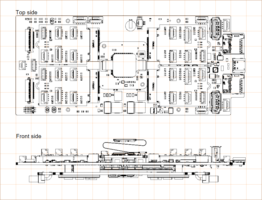
Simple assembly drawings do not contain much information beyond a 2D view of the PCBA. For example, a basic assembly drawigng shows the assembly layers with component outlines, reference designators, and the board outline. Typically, these are shown for the front and back sides (see below).

3D views in assembly drawings are also useful for an assembler to verify the intended look and feel of the completed PCBA, although these are not required. Typically, this will be an isometric or orthographic 3D view which provides perspective on the location and height of the components in the PCB assembly. Not all PCB design software offers support for these drawings in an automated way; the typical workflow is to export a 3D model, use MCAD software to extract a DXF of the 3D view, and then import the 3D view into a drafting tool like AutoCAD to create a PDF drawing. Altium Draftsman bypasses this workflow and creates the 3D view directly from your PCB layout file.
An alternative 3D view is to show the surface layer and side views, as shown below.
In the assembly drawing, we also have important specifications for the PCB assembler. At a high level, these include:
- The relevant qualification standard or quality standard for the assembly (most commonly IPC-A-610)
- Handling instructions or standards, e.g., for ESD protection, storage, and/or packaging
- Soldering requirements, including RoHS requirement or specific solder alloy and type
Some items, such as the application of thermal pads/TIMs, or the use of adhesives or underfills, may be identified as callouts in the assembly drawing. When using a callout, make sure to include a corresponding assembly note which clearly explains the purpose of the callout.
There is sometimes additional data needed for the assembly process which is not contained in the standard output files or drawings. These are outlined in the next section.
Additional Design Output Data
Some additional data that might be needed in manufacturing could include mechanical models or 3D prints, as well as MCAD data for an enclosure. The data required depends on the level of service being requested from the manufacturer and the scope of work. For example, in assembly, some radial or axial lead capacitors may need to be bent over on their side in a very specific orientation; your 3D prints and a STEP file can show this clearly. Other documentation includes prints, multiboard assembly instructions, packaging instructions, and wiring harness/cable assembly documentation.
MCAD Outputs
Output files are most commonly built for assembly with a PCB vendor, but some EMS companies may provide an enclosure assembly or box build service. To aid in these tasks, MCAD outputs might be requested. In particular, this could involve a 2D dimensioned drawing in DXF format showing mounting/fixation features, or it could be a full 3D model (e.g., STEP or Parasolid format).
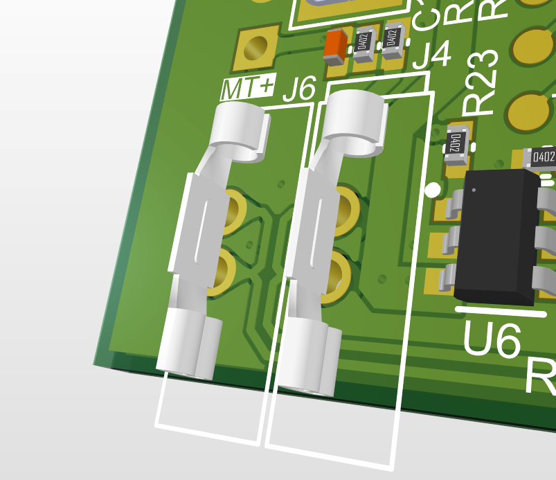
In some cases, viewing design data in a STEP file or as a 3D model in your PCB layout tool allows you to spot some DFM violations that may not be flagged by the online DRC engine. In the example is shown below, the connector outline on the silkscreen layer falls outside the board edge. When working in 2D mode in the layout editor, these defects types of can sometimes be missed, but they may be easier to spot in a 3D view.
Another specialized assembly requirement is with press-fit connectors or crimped connectors, which aren’t applied in a standard PCB soldering flow. Documentation on these components also needs to be provided; an assembly drawing or a specific requirements document might be the best place for this. If you’re unsure or you’re working with a new manufacturer, make sure to request this information and provide the right data accordingly.
Wiring Harnesses and Cabling
When your PCBA requires external connections through wiring harnesses or cable assemblies, additional documentation must be provided to the manufacturer. This typically includes cable assembly drawings that specify wire gauges, conductor counts, cable lengths, connector types and orientations, crimping specifications, and any required strain relief or protective sleeving. a wiring diagram or schematic showing the point-to-point connections between connectors will be required to ensure an assembler can build the wiring harness. These documents should also indicate any special requirements such as shielded cables, twisted pairs, color coding schemes, or labeling requirements.

Similar to PCB assembly drawings, wiring harness documentation should reference applicable quality standards (such as IPC/WHMA-A-620 for cable and wire harness assemblies) and include clear handling instructions, as well as testing instructions where applicable.
If the harness integrates directly with the PCBA through soldered wiring, press-fit terminals, or specific connector orientations, this interface information must be clearly communicated; this can be done with a callout in the main assembly drawing or the harness drawing. For products requiring both PCB assembly and cable assembly services, providing complete documentation upfront helps manufacturers understand the full scope of work and provide accurate quotes.
2D Assembly Views and 3D Isometric Views
Something that is quite useful in an assembly drawing are 2D and 3D views of the assembled PCB. 2D views can be constructed automatically from the data in the assembly layers, and this gives a view of the top and bottom sides of the assembled PCBA. 3D isometric views are constructed from the 3D models attached to your components. In the past, it was a specialized task to create all of these 3D models, attach them to components, and generate a 3D isometric view, but today's PCB design software can generate these views natively.
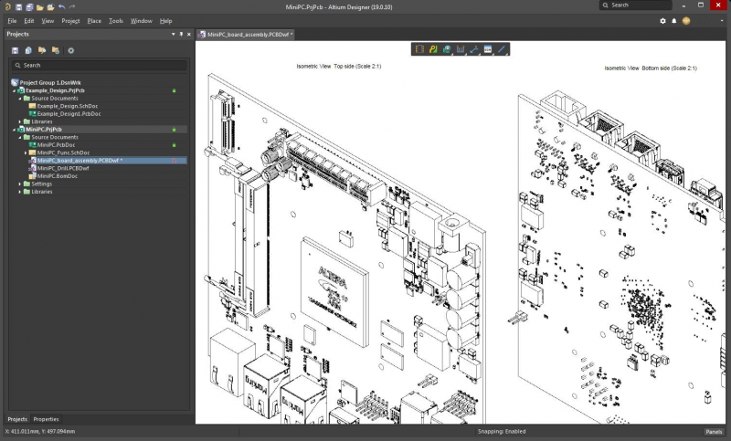
3D isometric views of the top side and bottom side of a PCB, shown in a Draftsman assembly drawing in Altium Designer.
Perspective views using the 3D models attached to your PCB components can also be generated in some PCB design software. Perspective views are used less often than 2D assembly layer views or 3D isometric views, but native 3D design features in PCB design software should enable quick creation of these views as needed in special situations.
Additional Design and Layer Prints
Finally, layer prints can be generated which will show specific layes (or combinations of layers) in a single file. A great example is to show silk and mask layers in a single print, which gives a way to quickly inspect surface layer errors before PCB fabrication. These prints can be useful for providing a potential assmebler/fabricator information about your design without sending the actual design files or the manufacturing files.
It's also common for engineering services companies to work with clients who are not PCB design experts or who do not have CAM software to review PCB manufacturing files. Layer prints showing the mask, copper, or silk layers can help users clients review or understand the design without doing a live walkthrough in the PCB layout software.

Readme File
Last but certainly not least is a readme file, which can be included with the remainder of your PCB design outputs. A readme file should be a simple text file that lists the important specifications you would normally put into a quote form. It is a summary of the major fab and assembly requirements, as well as the ordering information you want to communicate to a manufacturer. Readme files cannot be generated by your PCB design software; you will have to write it on your own after you complete the PCB design output package.
Whenever I receive a readme file in a design outputs package, it usually contains the following:
- Specific service level requested (turnkey, consigned, etc.)
- Quantities of PCBs to be ordered
- Board size and layer count
- Silkscreen and solder mask colors
- Any requirements for electrical testing
- Table of contents referencing and describing each Gerber file
- Any other build information not contained in a fabrication drawing
With a complete readme file, many basic questions that can delay the start of production can be addressed quickly. It may seem like a chore, but taking 15 minutes to prepare your readme file can save you days' worth of CAM review and production delays.
What Happens if Something is Missing?
Anytime documentation is missing or an important fabrication/assembly requirement is not specifically stated, your manufacturer will likely email you requesting the additional information. In some cases, such as cheaper prototype manufacturers, the company will go with some “standard” capability and requirement that is applicable to most basic designs. If you aren’t worried about things like surface platings or tenting, then just focus on creating the main fabrication files and leave the rest up to your manufacturer. Different companies offer different levels of service and will be willing to help you get your first PCBA manufactured successfully.
Summary
In the past, designers had to prepare PCB design output files and manufacturing data by hand, which required compiling information from multiple design documents and manually preparing final deliverables. Today’s design tools can help you prepare this data package automatically so that you can save time and get through design reviews quickly. Next time you’re planning a new project, use the best CAD tools to help you quickly create a PCB layout and prepare it for production.
Once you’ve finished your PCB layout and you’ve completed a thorough design review, it’s easy to generate PCB design output files for your design in Altium Designer®. The OutJob file feature lets you create manufacturing file templates for your projects and quickly generate groups of files from your PCB layout and schematic data. When you’re ready to release these files to your manufacturer, the Altium 365™ platform makes it easy to collaborate and share your projects.
We have only scratched the surface of what’s possible with Altium Designer on Altium 365. Start your free trial of Altium Designer + Altium 365 today.
Frequently Asked Questions
What PCB design output files are required for manufacturing?
A complete manufacturing package typically includes Gerber, ODB++, or IPC-2581 fabrication data, NC drill files, a bill of materials, pick-and-place data, fabrication and assembly drawings, and an IPC-D-356 netlist. Complex products may also require STEP models, testpoint reports, firmware binaries, test procedures, or cable documentation.
Why is an IPC-D-356 netlist included with PCB manufacturing data?
The IPC-D-356 netlist gives the fabricator a standardized point-to-point description of the PCB connectivity. It allows CAM software to detect shorts or opens that cannot be identified from Gerber image data alone and helps define probe locations for bare-board electrical testing.
Should you use Gerber, ODB++, or IPC-2581 files for PCB manufacturing?
Gerber files remain the safest option because they are accepted by nearly every PCB fabricator. ODB++ and IPC-2581 can consolidate fabrication, assembly, netlist, and test data into a single package, but support varies, so designers should confirm the manufacturer’s preferred format before release.
What information belongs in a PCB assembly drawing?
A PCB assembly drawing should show the board outline, component outlines, reference designators, component orientation, and top and bottom assembly views. It should also include assembly standards, soldering requirements, handling instructions, and callouts for adhesives, underfill, thermal interface materials, or other special processes.

About Author
Related Resources
Related Technical Documentation
Table of Contents
- The Standard List of PCB Design Output Files
- It Starts With PCB Fabrication Files
- Gerbers vs. Intelligent Output Formats
- PCB Assembly Outputs
- Additional Design Output Data
- MCAD Outputs
- Wiring Harnesses and Cabling
- 2D Assembly Views and 3D Isometric Views
- Additional Design and Layer Prints
- Readme File
- What Happens if Something is Missing?
- Summary
- Frequently Asked Questions
Design to Release, Without the Friction
- Keep reviews tied to the right version
- Reduce handoff confusion and rework
- Spot sourcing and release risk earlier
- Work solo, share when needed
Get Started
Thank you, you are now subscribed to updates.