Articles and resources related to PCB Layout: Pads & Vias. Check out Altium.com to learn more about PCB Layout and other relevant topics.
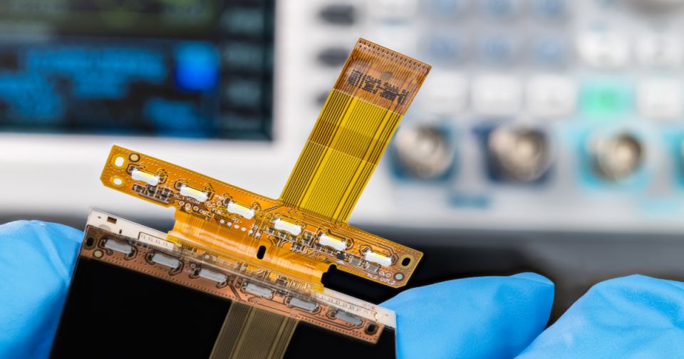
When space is tight, via-in-pad in rigid-flex demands filled vias, clean stackups, and stress control. Learn when to use VIP and when to skip it.
PCB design tips for reliable vias. Learn how via types, copper filling, and fabrication choices improve board reliability and manufacturability.
If you work in the electronics industry or in research, there’s a chance that simulations are a regular part of
Stitching vias are more than just periodic via arrays, they provide groups of net connections across layers that are needed in power, RF, high-speed, and more.
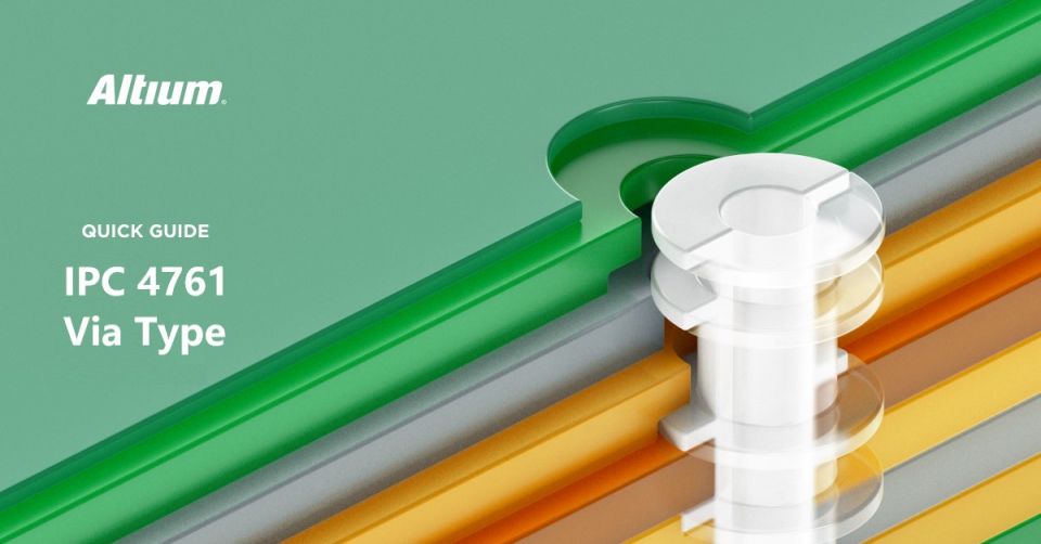
The document describes the possibilities of supporting several types of adapter protection according to the standardized IPC-4761 via types in Altium with the advantages and disadvantages of each.
Take a look at the above image of a PCB layout, specifically the vias and drill holes poking through the
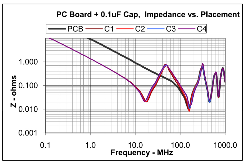
Take a look at traditional PDS impedance versus the “energy flow” view of PDS design. We’ll debunk misleading information that could cause your designs to fail.