Skip to main content
Mobile menu
产品
Altium Designer
广泛使用的PCB设计解决方案
Altium 365
基于云原生架构的电子产品研发协同平台
For Parts and Data
大量简单易用的元器件数据库
Altium Develop
资源 & 支持中心
Altium 365 免费工具
Gerber Compare
在线 PCB 查看器
了解产品
下载
联系我们
关注微信
扫描二维码
关注Altium微信平台
资源 & 支持中心
博客
支持中心
文档
Altium Community
社群
Bug提交
创意
教育项目
专业培训/认证
大学/学院学生
大学/学院教育工作者
资源中心
Education & Training
Student Lab
Educator Center
Altium Education Curriculum
Altium Professional Training
Search Open
Search
Search Close
帮助
Home
Main Chinese menu
首页
PCB设计
团队协作
元器件创建
PCB数据管理
PCB设计输出和文档
ECAD/MCAD
HDI设计
高速设计
多板设计
PCB布局
PCB布线
PCB供应链
电源完整性
RF设计
刚柔结合板PCB设计
原理图输入
信号完整性
PCB设计仿真/分析
软件
Altium Designer的
资源中心
工程新闻
指南书
网络研讨会
Overview
All Content
CoDesign and CoEngineering (ECAD/MCAD Collaboration)
Component Management and Libraries
Data Management and Version Control
Manufacturing Outputs and Compliance
PCB Design and Layout
Supply Chain and Component Sourcing
Systems and Product Design
Filter
清除
Role
全部
ECAD Librarians
Electrical Engineers
Engineering Managers
IT Managers
Mechanical Designers
PCB设计
Procurement Managers
Software Engineers
Software
全部
Develop
Agile
Altium Designer的
Altium 365
Assembly Assistant
BOM Portal
PLM集成
GovCloud
Jira Integration
Octopart
Requirements Portal
SiliconExpert
Z2Data
Content Type
全部
指南书
影片
网络研讨会
播客
白皮书
Region
全部
Edgewater Research: Electronics Supply Chain Weekly Digest June
12 min
Sponsored
June 16, 2023 Important Disclosures in the Appendix A weekly collection of news summaries, survey results and channel insights, and
阅读文章
离散半导体的5大趋势:新动态与未来展望
1 min
What's New
半导体是技术世界中不为人知的英雄。它们在幕后工作,应用于从玩具和智能手机到汽车和恒温器的各种设备中。它们还使得如人工智能和机器学习等突破性技术成为可能。 但并非所有半导体都是平等创造的。有些是离散的,意味着它们是执行基本电子功能的单一设备。其他则是集成的,意味着它们由单一芯片上的许多设备组成,执行复杂功能。 离散半导体执行的基本功能包括整流( 二极管)、放大( 晶体管)和开关(晶体管和 晶闸管)。离散器件通常有两个或三个端子。它们可能看起来简单,但对于许多需要高性能、低功耗和更大功能性的应用而言,它们是必不可少的。它们还提供比集成电路(ICs)更多的灵活性和定制性。 离散半导体市场正在蓬勃发展。 预计从2021年到2027年,其复合年增长率(CAGR)为6.3%,到2027年市场规模将达到370亿美元。市场增长是由工业、消费电子、信息技术和电信、汽车及其他应用中对离散半导体需求增加所驱动的。 塑造离散半导体未来的趋势 在本文中,我们将探讨五大趋势,这些趋势正在塑造离散半导体的未来,以及电子工程师如何在其设计中利用这些趋势。这些趋势是人工智能(AI)、先进材料、先进封装、新颖架构和物联网(IoT)。让我们深入了解! 人工智能 AI需要离散半导体具备智能化、高效率以及处理大量数据和计算的能力。离散半导体通过使用先进材料和架构实现这一点,从而实现更高速度、更低功耗和更大的功能性。 例如, 智能传感器可以使用AI算法在本地处理数据,并与其他设备或云通信,而边缘计算设备可以在不依赖云的情况下在网络边缘执行AI任务。 先进材料 先进材料——包括氮化镓(GaN)、碳化硅(SiC)和有机电子学——与传统材料(即硅、锗和砷化镓)相比具有优越的性能和性能。先进材料可以通过提高效率、可靠性、速度和功率密度来增强离散半导体的性能和功能。 例如,由GaN和SiC制成的组件可以承受比硅更高的电压、温度和频率。它们减小了电动汽车、可再生能源和数据中心等应用中电源转换器的尺寸、重量和成本。 有机电子学可以实现灵活、轻便和低成本的光电设备,如有机发光二极管(OLED)、有机太阳能电池和有机激光器。与传统光电设备相比,它们提供了更好的颜色质量、更宽的视角和更低的功耗优势。 新颖架构 新颖架构是设计和集成离散半导体的新方法,提供比传统架构更高的功能性和性能。这些架构包括三维(3D)集成、芯片组和
阅读文章
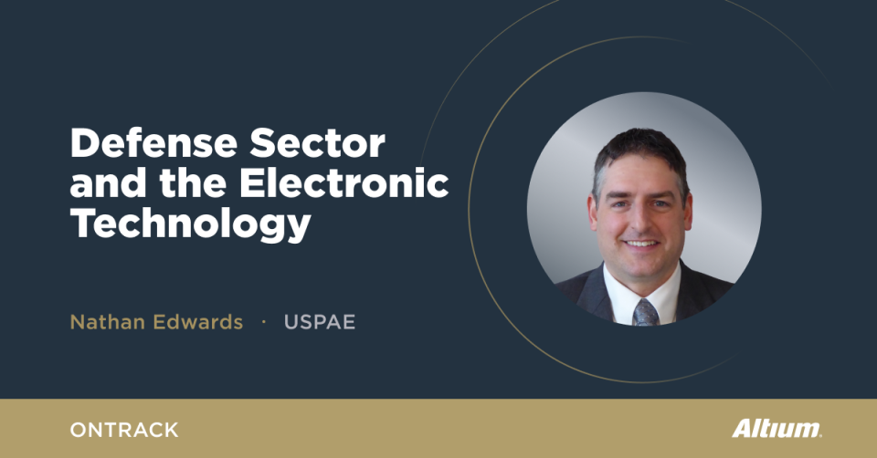
The Impact of the Defense Sector in the Electronic Industry Ecosystem
44 min
Podcasts
Contractors / Consultants / Service Bureaus
Our guest Nathan Edwards, an Executive Director, U.S. Partnership for Assured Electronics (USPAE) will share with us what goes in a Defense Electronic Consortium (DEC) and how all of these impact the electronics eco-system.
阅读文章
Understanding the PCB Supply Chain
11 min
Blog
Global supply chains are an intricate web of processes and stakeholders involved in the design, manufacture, assembly, and distribution of
阅读文章
Should a Capacitor Be Used For ESD Protection?
11 min
Blog
Electrical Engineers
PCB设计
Engineering Specialists
Capacitors are not capable of fully protecting a system from ESD, other components are also needed for comprehensive protection.
阅读文章
Why Are Advanced Car Radars Using So Many Antennas?
7 min
Blog
Electrical Engineers
Advanced car radar systems rely on large virtual arrays for high-resolution imaging, long range, and/or tracking of multiple objects.
阅读文章
The Current State of AI in PCB Design in 2023
7 min
Blog
PCB设计
Electrical Engineers
Your favorite machine learning, optimization, and generative AI algorithms may soon be used in your favorite PCB design program. Now
阅读文章
Pagination
First page
« First
Previous page
‹‹
页面
161
当前页面
162
页面
163
页面
164
页面
165
页面
166
Next page
››
Last page
Last »


 沪公网安备 31010502006411号