

高速PCB设计
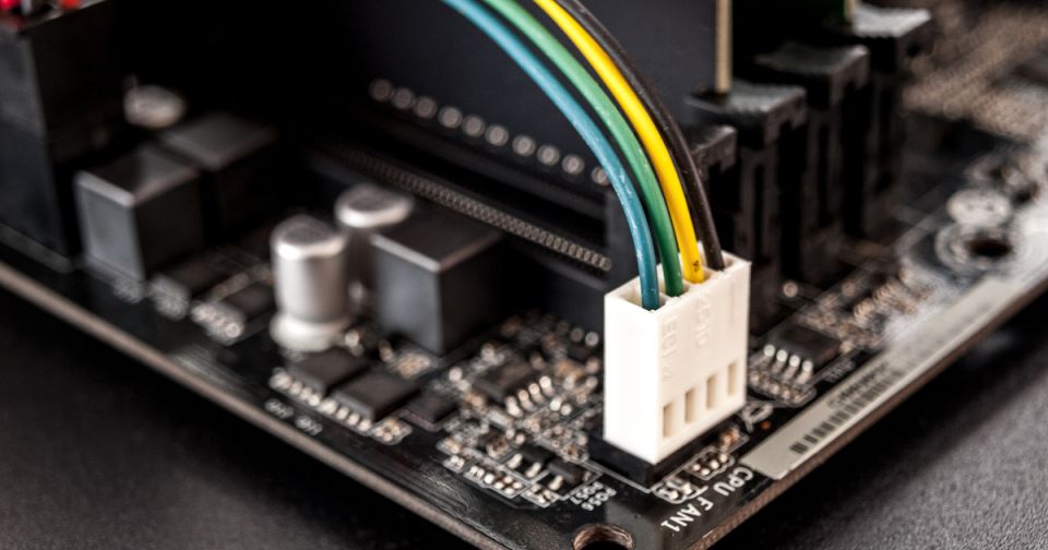
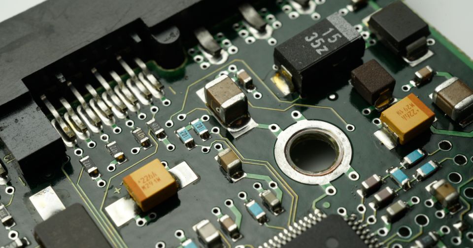
高速PCB设计使用具有快速边沿的信号,其中设备切换状态的速度如此之快,以至于在信号完成元件间的传输之前便已完成过渡。高速PCB设计中的互连需要精确的阻抗匹配,布线应考虑互连沿线的潜在损耗、失真、EMI和串扰。正确的传输线设计、布局和布线有助于最大限度地减少这些问题。浏览我们的资源库,详细了解印刷电路板中成功的高速电路板布局和传输线设计。
指南
Explore Guidebooks for High Speed Design and start creating today!


网络研讨会
Explore upcoming and on-demand webinars for High Speed Design.

视频
Watch videos for High Speed Design to learn more!


Customer Success Stories
Discover customers finding success with Altium's High Speed Design solutions!


Technical Documentation
Explore Technical Documentation related to High-Speed Design

Articles
Explore more popular content for High Speed PCB Design!

 沪公网安备 31010502006411号