Skip to main content
Mobile menu
产品
Altium Designer
广泛使用的PCB设计解决方案
Altium 365
基于云原生架构的电子产品研发协同平台
For Parts and Data
大量简单易用的元器件数据库
Altium Develop
资源 & 支持中心
Altium 365 免费工具
Gerber Compare
在线 PCB 查看器
了解产品
下载
联系我们
关注微信
扫描二维码
关注Altium微信平台
资源 & 支持中心
博客
支持中心
文档
Altium Community
社群
Bug提交
创意
教育项目
专业培训/认证
大学/学院学生
大学/学院教育工作者
资源中心
Education & Training
Student Lab
Educator Center
Altium Education Curriculum
Altium Professional Training
Search Open
Search
Search Close
帮助
Home
Main Chinese menu
首页
PCB设计
团队协作
元器件创建
PCB数据管理
PCB设计输出和文档
ECAD/MCAD
HDI设计
高速设计
多板设计
PCB布局
PCB布线
PCB供应链
电源完整性
RF设计
刚柔结合板PCB设计
原理图输入
信号完整性
PCB设计仿真/分析
软件
Altium Designer的
资源中心
工程新闻
指南书
网络研讨会
Overview
All Content
CoDesign and CoEngineering (ECAD/MCAD Collaboration)
Component Management and Libraries
Data Management and Version Control
Manufacturing Outputs and Compliance
PCB Design and Layout
Supply Chain and Component Sourcing
Systems and Product Design
Filter
清除
Role
全部
ECAD Librarians
Electrical Engineers
Engineering Managers
IT Managers
Mechanical Designers
PCB设计
Procurement Managers
Software Engineers
Software
全部
Develop
Agile
Altium Designer的
Altium 365
Assembly Assistant
BOM Portal
PLM集成
GovCloud
Jira Integration
Octopart
Requirements Portal
SiliconExpert
Z2Data
Content Type
全部
指南书
影片
网络研讨会
播客
白皮书
Region
全部
43:11
Altium 365 webinar series | Collaborating with Contractors
1 min
Webinars
We are pleased to offer a 3 part Altium Academy Virtual series to discuss the problems that companies can encounter
阅读文章
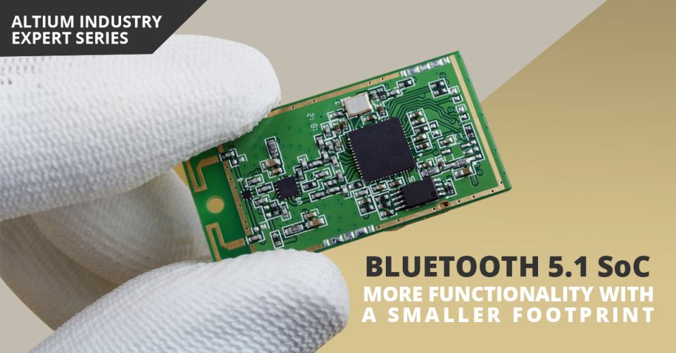
Bluetooth 5.1 SoC vs. Module: Which is Best for Your Design?
5 min
Thought Leadership
The list of features available in Bluetooth just got a little longer since the release of Bluetooth 5.1. Component manufacturers
阅读文章
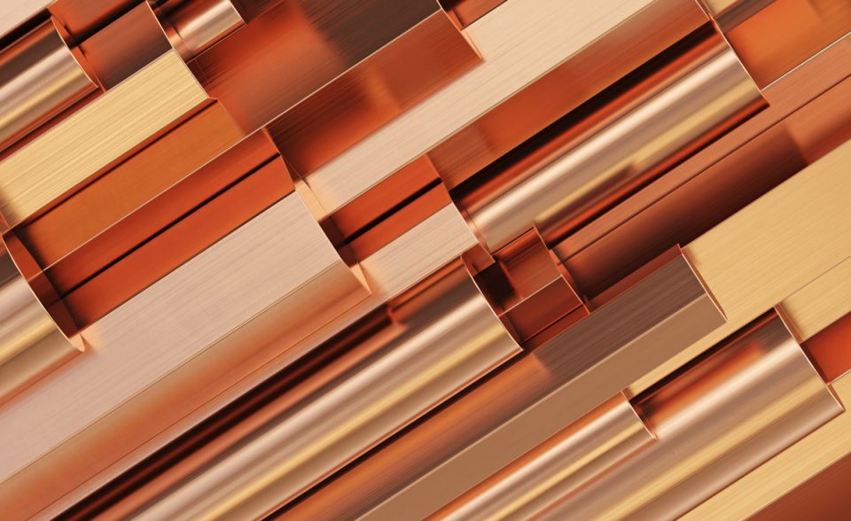
How Copper Foil Roughness Affects Your Signals and Impedance
9 min
Blog
The history of engineering, both electrical and mechanical, is littered with approximations that have fallen by the wayside. These approximations
阅读文章
Exploring Lead Time & Updated Specs View
5 min
What's New
Welcome to Octopart’s Specs View Did you know that Octopart has more than one search results view? Specs View makes
阅读文章
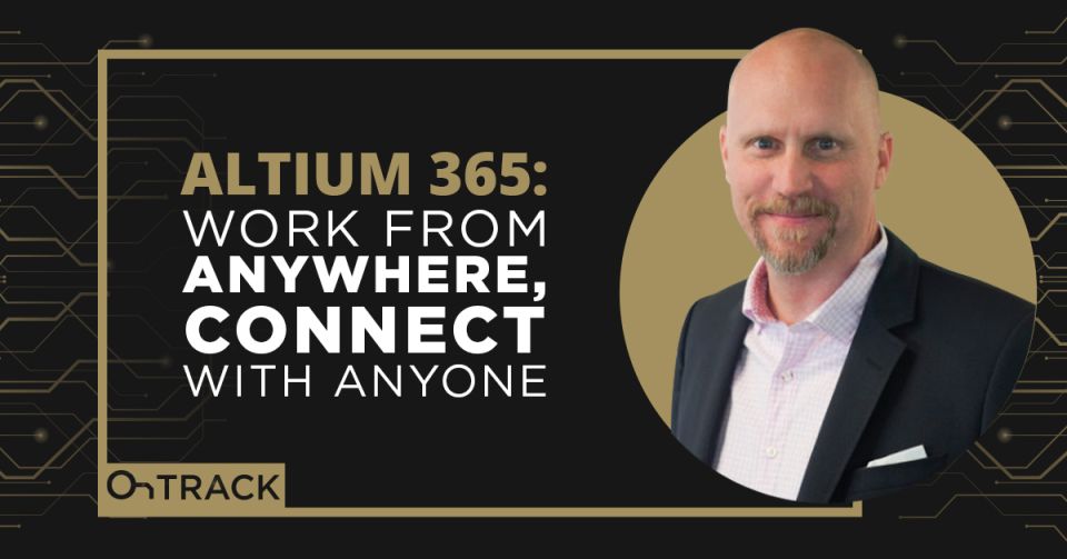
Altium 365: Work from Anywhere, Connect with Anyone
2 min
OnTrack
Altium 365 has launched in the midst of a worldwide quarantine effort. Lawrence Romine explains how the launch timing couldn’t be more serendipitous.
阅读文章
2:20:16
Atium Academy Virtual Session: Component Creation
1 min
Webinars
Watch our webinar on Component Creation as part of the Altium Academy Series.
阅读文章
CCD与CMOS传感器比较:哪个更适合成像?
1 min
Guide Books
在这台相机中应该使用CCD还是CMOS传感器?这里是如何比较这些传感器的方法。 任何用于成像、计算机视觉和光子学应用的设计都需要某种类型的光学组件和传感器才能正常工作。你的下一个光学系统将整合广泛的光学组件,而成像传感器是光学和电子世界之间的桥梁。 明智的传感器选择需要考虑许多因素。这些因素包括响应时间、外形尺寸、分辨率和应用等。在CCD与CMOS传感器之间的选择可能很难,但它将决定你的系统解析图像的速度,同时避免饱和。如果你需要在可见范围之外工作,你将需要考虑使用Si以外的替代材料以实现有效成像。在某些应用中,使用光电二极管阵列可能更有意义。这里是你需要了解的关于这些不同类型的传感器以及如何为你的应用选择正确组件的信息。 成像传感器和系统要求 任何成像系统都应该设计以满足一些特定的要求,其中许多要求都围绕光学传感器的选择。首先,考虑你的波长范围所需的材料,然后比较分辨率、响应时间和线性等方面。 活性材料和检测范围 你的传感器中使用的活性材料将决定敏感波长范围、带尾损失和温度敏感性。根据你的应用,你可能在红外、可见光或紫外范围工作。对于相机系统,你会希望在整个可见范围内都有灵敏度,除非你正在研究热成像系统。对于专门的成像应用,如荧光成像,你可能在从红外到紫外的任何范围内工作。 一些活性材料仍处于研究阶段,而一些已作为商业化组件可用。如果你在比较CCD与CMOS传感器组件,活性材料是选择候选传感器时的一个好的起点。 Si: 这是成像传感器中最常用的材料。其间接带隙为1.1 eV(~1100 nm吸收边缘),最适合可见光和近红外波长。 InGaAs: 这种III-V材料提供了直到~2600 nm的红外检测。其低结电容(1 nF)使InGaAs传感器非常适合于SMF波长(1310和1550 nm)的应用。通过改变In(1-x)GaxAs的化学计量比来实现调谐。市场上有光子学供应商提供的InGaAs CCD传感器,像IBM这样的公司已经展示了InGaAs与CMOS工艺的兼容性。 Ge: 由于其成本高于Si,这种材料在CCD相机和传感器中较少见,而全Ge和SiGe
阅读文章
Pagination
First page
« First
Previous page
‹‹
页面
370
当前页面
371
页面
372
页面
373
页面
374
页面
375
Next page
››
Last page
Last »


 沪公网安备 31010502006411号