


PCIe Routing with AC Coupling Capacitors

At a Glance
AC coupling capacitors remove DC offset so that high speed PCIe lanes can operate properly. Learn more about PCIe AC coupling capacitor selection and placement.


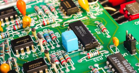
Coupling capacitors find plenty of uses in analog applications and on differential protocols, acting essentially as high pass filters that remove DC bias carried seen on a signal. In PCIe routing, coupling capacitors are used for the same function (removing DC offset), but for different purposes. In the case of PCIe routing, there are a few reasons to place AC coupling capacitors on differential pairs beyond the fact that AC coupling capacitors are listed in the standard. In this article, we’ll look briefly at where to place coupling capacitors on PCIe links, as well as the reasons these are placed on PCIe links.
PCIe Routing: The Role of AC Coupling Capacitors
All PCIe lanes are routed as differential pairs with defined differential impedance, and the Tx side of a lane requires AC coupling capacitors. According to the PCIe specification, there are three main reasons to place coupling capacitors on the Tx lines:
- DC isolation: Even though PCIe differential pairs are being routed over a continuous ground region, there needs to be DC isolation between the driver and receiver sides of a lane. Since the differential signal is recovered by measuring the potential difference between the pairs, the AC caps remove any DC offset induced on the signal when a driver and receiver run at different voltages.
- Detecting plug/unplug events: Some add-in cards or modules are hot-swappable. The capacitors on a Tx pair allow the driver to use an RC time constant to detect the presence of a receiver at the end of a lane.
- Detecting the lane count: In components that have multiple PCIe lanes, the plug/unplug events will occur across each lane, and the number of triggered lanes can be sensed by the PCIe-capable device.
- Block ground offset: The corollary to the first point above is factoring out any ground offset between a motherboard and a PCIe add-in card. The capacitor eliminates the influence of any DC offset between the ground regions in the main board and the add-in card or module.
The caps also need to pass as much signal as possible up to high frequencies, meaning they should have high enough self-resonant frequency. The original specification requires at least the 3rd harmonic above the fundamental, which can reach into the GHz regime for newer PCIe generations. When a signal reaches the receiver, its chances of successful recovery will be higher when higher bandwidth is available, so the passband for these caps should have sufficiently high cutoff.
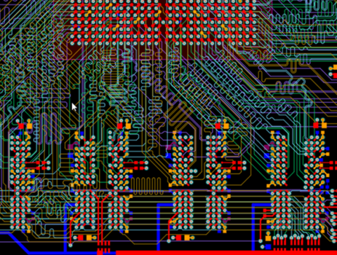
PCIe AC Coupling Capacitors Placement
The PCIe Base Specification requires that each lane of a PCIe channel be AC-coupled between the driver and receiver for the above reasons. The actual location of the AC coupling capacitors can be located either on or off the die/component at each end of the link. In other words, if you look at a random layout and you don’t see AC coupling capacitors along the link, they may be embedded in the I/Os on the transmitter die. Make sure to check the datasheets for your components to verify this.

In most cases, the AC coupling capacitors are not built into the transmit side of the interface, so AC caps need to be placed somewhere along the link. Where these are placed depends on the system being designed. These are summarized in the table below.
|
|
|
|
|
|
|
|
|
Routing on Top or Bottom Layers?
One good strategy for working with PCIe interfaces is to route Rx and Tx lanes on opposite layers of the board. Many PCBs that will contain PCIe lanes will have four layers. For example, computer motherboards and add-in cards are commonly optimized for low layer count to reduce costs, which dictates a 4-layer board (SIG + PWR/GND/GND/SIG + PWR stackup). In this type of system, routing across vias will be possible without stubs that might limit channel bandwidth. Whichever layer you decide to route on, it’s best to place caps and route on the surface layer so that the via inductance does not limit the channel bandwidth.
Don’t Forget to Evaluate PCIe Links!
Although PCIe AC coupling capacitor placement is listed in the PCI-SIG standard, it’s still important to fully evaluate the link design in your system. PCIe capacitor placement is just part of the story in PCIe routing. When working at high speeds in newer PCIe generations, evaluation is also important to ensure the link works properly. This requires testing and simulation at minimum.
Simulation tools make it easy to evaluate a PCIe channel by looking at a few key metrics:
- An eye diagram for each lane
- An impedance simulator that can spot impedance deviations along a lane
- S-parameter simulators for each lane
With PCIe links being broadband digital channels, they require examination of signal behavior directly from an eye diagram and evaluation of bit error rate to determine compliance. If routing from an expansion card onto a system host board via a through-hole connector, you will also need to qualify stubs along the routes. Read this article on identifying stub resonances in PCIe links to learn more.
When you need to evaluate your design in a comprehensive simulation-driven workflow, use the complete set of PCB design, layout, and simulation features in Altium. When you need to examine signal integrity problems and extract S-parameters from your systems, you can use the EDB Exporter extension to import a design into Ansys field solvers and perform a range of SI/PI simulations. The export options from Altium also support other field solvers, such as the specialized Simbeor solver for interconnect evaluation. When you’ve finished your design, and you want to release files to your manufacturer, Altium makes it easy to collaborate and share your projects.
Reach out to one of our experts for more information on PCIe routing with AC coupling capacitors.

关于作者
Related Technical Documentation
相关资源
目录
从设计到发布,全程无阻碍
- 让评审始终关联到正确的版本
- 减少交接中的混乱和返工
- 更早发现采购与发布风险
- 可独立工作,按需共享
开始使用
Thank you, you are now subscribed to updates.


 沪公网安备 31010502006411号