


Best PCB Routing Practices after Auto Routing Goes the Distance

At a Glance
PCB auto-routing and routing techniques that will help you to finish your PCB layout once the auto-routing is completed.


Right at the outset of this article, I'll make one thing clear: I personally do not use an auto-router. One of the designers who works for me sometimes use it and only on targeted component groups that are difficult to mess up. But for everything else that matters, particularly digital interfaces and RF transmission lines, auto-routing usually doesn't cut it.
Auto-routers are tools that take a fair amount of configuration, just like any other tool. If you're a designer that does use auto-routers, and you've figured out a configuration and workflow that helps you be more productive, then I say kudos. Not everyone has the patience for it, and I think engineers can be control freaks regardless.
But if you are considering using an auto-router, how should you manage and control the tool within your workflow? Building a productive workflow around auto-routing is just as important as configuring the auto-router tool itself. If we start to see more AI tools that also perform a version of auto-routing, these tools will also need to be brought into a workflow in a way that ensures productivity. If this sounds like you, then here are some tips that can help you out.
Global or Local Auto-Routing?
The designers I've talked to that use auto-routing have told me they get the best results when they stay local. In other words, they only pick small groups of components, and they will only auto route on that group. If a group can be routed using only traces on the same layer, or possibly with one layer change, then that's okay. The smaller the group selected, the less clean up there will be once the auto-router completes.
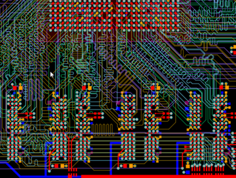
Image small group of auto-routed components
I have found that larger groups of components with more complex rule sets and constraints could result in more cleanup once the auto-router completes. If you request the auto-router to start making complex decisions, such as attempting to determine when to change layers, the auto-router might not see the full range of tradeoffs and it could make a poor decision.
For example, take a look at the route below. There are several groups of long traces that belong to the same net class, and one of these involves a layer transition in order to make a complete connection. Due to the placement of this via for the layer transition, the net right next to it now has to route a very tight run around the via.

Of course, this roundabout route to avoid the via probably could have also been achieved in a much cleaner way with its own via. But for whatever reason, the auto-router did not select that option, probably due to some other trace on a different layer. Because auto-routers are a bit of a black box in terms of their core algorithm, it can be difficult to infer how exactly the tool makes those decisions. Also, because the endpoints of these routes were far from each other, I think it makes more sense to do those traces manually anyways.
Another example of cleanup is odd acute angle routes such as that shown below. Over 90% of designs will not experience any noticeable degradation due to this right-angle routing, but most designers will look at this and will prefer to clean up the route.

Before and After Auto-Routing
Clearly, the use of auto-routing requires carefully choosing the components and nets you want to auto-route in order to minimize cleanup. I think there are a few ways to organize or group components in order to create circuit blocks for auto-routing:
- Use net classes or component classes to group components
- Use Rooms to designate groups of components and select only within a room
- Group components only by their proximity to each other in the PCB layout
- Do sequential importing of components into a blank PCB one schematic sheet at a time
The last strategy is sometimes one that I use just to get groups of parts into a board as it eliminates the need to cross-probe to the schematic just to make sure I am keeping parts in the same circuit. The other methods of grouping components or nets are also helpful for keeping you organized in general.
Once everything is grouped together, you can usually see what might be good candidates for auto-routing right after placement. Pick the appropriate auto-routing strategy for different groups of components and give the auto-router a try. If it does not produce a result that you like, you can always hit Ctrl+Z and undo the auto-routing.
Once auto-router completes, you'll have some cleanup to do and you will have to draw out any large rails in the board. This is some of the final cleanup that is needed to keep a board looking clean and organized, as well as ensure it is functional. For high-speed digital nets and RF nets, those will need to be handled by hand just because they can be sensitive to length, proximity to other nets, proximity to copper pour, and the number of layer transitions through vias.
Auto-Interactive Routing is the Best of Both Worlds
If you have a lot of traces to route and you want to speed up the process, Auto interactive routing gives you the best balance between Automation and control. Like I said earlier, Engineers can sometimes be control freaks, but that is what's needed to ensure you get the best possible products. Auto interactive routing gives you that control while filling in the Minor Details that would normally be routed by hand.

Additional routing tools or features that help you stay productive are glossing, component retracing, and differential pair routing. These tools give you everything you need to stay maximally productive and build advanced products, whether you have just a few nets or thousands of nets to route. To design advanced products, PCB designers trust the cutting-edge features in Altium Designer®. When you’ve finished your design, and you want to release files to your manufacturer, the Altium 365™ platform makes it easy to collaborate and share your projects.
We have only scratched the surface of what’s possible with Altium Designer on Altium 365. Start your free trial of Altium Designer + Altium 365 today.

关于作者
Related Technical Documentation
相关资源
目录
从设计到发布,全程无阻碍
- 让评审始终关联到正确的版本
- 减少交接中的混乱和返工
- 更早发现采购与发布风险
- 可独立工作,按需共享
开始使用
Thank you, you are now subscribed to updates.


 沪公网安备 31010502006411号