


Ceramic vs. FR4 Multilayer PCBs: When to Use Either and How


Ceramic materials electronics are specialty materials used as PCB insulators and as substrates for IC packages. Today, ceramic production capacity for PCBs is easy to access from overseas vendors, and these materials see significant use in aerospace and automotive industries.
Ceramic PCBs offer particular advantages over FR4 boards, although there is no single “ceramic” material. The current set of commercialized ceramic materials for PCBs are alumina (Al2O3), aluminum nitride (AlN), beryllium oxide (BeO), boron nitride (BN), and silicon carbide (SiC); the first three in this list are most common as their fabrication procedure has been adapted from the IC packaging world.
If you’re considering when to use a ceramic PCB substrate instead of a standard FR4 PCB, read this guide to learn more about the usage of these materials.
Ceramic vs. FR4 Material Properties
There are two big differences between ceramic materials and epoxy-resin materials (such as FR4 or related organic materials):
- Thermal conductivity
- Dielectric constant
- CTE value
- Mechanical rigidity
Obviously there are other material differences that affect processing and operation, such as differences in dielectric constant, CTE value, and glass transition temperature. But for the most part, the main selection criteria that drives usage of ceramic PCBs is the above two material properties.
Thermal Conductivity
The biggest difference between FR4 and ceramic materials is their thermal conductivity. FR4 has very low thermal conductivity compared to the ceramic materials used for a circuit. If you are familiar with chemistry and physics, you may know that thermally conductive materials tend to also be good electrical conductors. Ceramics buck this trend, meaning their electrical conductivity is still low enough that these boards can be used for PCB substrates.
|
Ceramic material |
Thermal conductivity |
|
Alumina |
~20x FR4 |
|
Aluminum nitride and silicon carbide |
~100x FR4 |
|
Beryllium oxide and boron nitride |
Greater than 100x FR4 |
Dielectric Constant
Dielectric constant values for ceramics generally vary wildly from very low values to very high values. For example, the only way small case ceramic capacitors can reach meaningful capacitance values is with ceramics that have very high Dk values. Similarly, in PTFE laminates, ceramic fillers are used to tune the dielectric constant of the material
|
Ceramic material |
Dielectric constant |
|
Alumina |
9.0 to 10.0 |
|
Aluminum nitride |
8.6 to 9.0 |
|
Silicon carbide |
~9.66 (Cubic SiC: ~9.72) |
|
Beryllium oxide |
~6.76 |
|
Boron nitride |
3.3 to 3.8 at low frequencies |
Aside from boron nitride, all the values presented above are higher than FR4 dielectric constant and are comparable to some ceramic-filled PTFE laminates used in RF devices. The higher-Dk ceramic materials can be useful in many instances, such as in RF systems requiring printed circuits operating at low frequencies. In these devices, a higher Dk value allows the physical size of the circuit to be smaller because signal wavelengths are smaller when Dk is larger.
The point not mentioned above is loss tangent and dispersion, which can very significantly. Loss tangent data in various frequency ranges can be found in the research literature, some of which is free online. Note that the dispersion can be very large for ceramic materials; for example, in boron nitride, the dielectric constant rises to ~4.5 near 9 GH, a level of dispersion which is significantly larger than what is seen in FR4 laminates.
Multilayer Ceramic PCB Manufacturing
1. Tape Casting and Hole Formation
First, ceramic powders are mixed with organic binding agents and cast into the board shape with tape. This is a doctor blade process with a stencil (can be a taped stencil) that allows the thickness to be controlled within a specific stencil area. Once the ceramic slurry dries and hardens, holes are punched into the unfired ceramic to form room for vertical interconnects. Via sizes in ceramic substrates can be of similar size as those used in organic substrates.
2. Metal Paste Screen Printing
The metallization process for ceramic PCBs requires the use of a conductive paste to define traces and vertical interconnects in each layer (usually silver or gold paste). Copper pastes are also available for screen-printed electronics (such as transparent PET substrates); contact your manufacturer if copper is a preferred material. For fine-line designs on ceramic substrates, the printed feature size and resolution will be limited by the screen printer’s capabilities.

3. Stackup and Co-firing
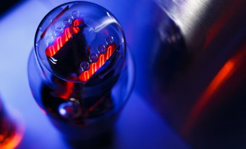
Once the ceramic layers have been printed, they are stacked in the appropriate order and the entire stack is fired in an oven. The firing temperature required to bake the ceramic board can reach near 1000 °C, which matches the sintering temperature of the material of gold and silver pastes. Multiple ramp and soak cycles may be required to fully crystallize the ceramic material to its required crystal state. Once completed, the fabricated PCB can have a solder mask applied, and it will be inspected before assembly.
![]()
Your ceramic PCB might be fired in an oven like this
To summarize, there are a few major instances where ceramic PCBs are desirable:
- In very high temperature operating environments, where the PCB will act like a heat spreader
- In environments where the mechanical rigidity is needed to withstand vibration
- In RF systems where smaller circuit sizes are desired at low frequencies
The extensive design, simulation, and analysis features in Altium Designer® give you the power to build PCBs from any material, including ceramics. Now you can download a free trial and find out if Altium Designer is right for you. Talk to an Altium expert today if you want to learn more.

关于作者
相关资源
目录
从设计到发布,全程无阻碍
- 让评审始终关联到正确的版本
- 减少交接中的混乱和返工
- 更早发现采购与发布风险
- 可独立工作,按需共享
开始使用
Thank you, you are now subscribed to updates.


 沪公网安备 31010502006411号