


Prevent Copper Wear and Short Circuits with Rules-Driven Design


The phrase “PCB design” might seem to emphasize design, but it actually includes all aspects of printed circuit board manufacturing. Without the proper attention to design for manufacturability (DFM), a design might be sent back to a designer for corrections and further review by a CAM engineer. DFM is meant to ensure a board can be produced with high yield and is best implemented in rules-driven design software. When you need to follow important DFM requirements and ensure your circuit board functions correctly, use the rules-driven design rules in Altium Designer.
ALTIUM DESIGNER
The right design software allows you to specify test conditions for detecting shorts during fabrication.
A short circuit in your PCB is a simple defect, but it can cause your board to fail completely. Most routing defects will be found in the validation stage, while the simulation stage will ensure a quality signal is strong and maintained. Testing needs to occur during fabrication and assembly to ensure your circuit board’s electrical behavior matches the design specifications.
The first and most notable feature in Altium Designer is rules checks to ensure you maintain clearances required to prevent short circuits. The concept is simple: Altium Designer checks a handful of rules as you route traces in your PCB layout, which can identify open and short circuit errors during the design process. To aid fabricators, you can also define testpoints in your board so that in-circuit testing can be performed. Only Altium Designer includes these important verification features alongside a set of world-class tools for circuit board design.
Identifying Short Circuits in Your Circuit Board
Short circuits can arise accidentally for a number of reasons, and the list is too long to place in this article. However, some of the most common causes of short circuits are accidental bridging during fabrication and assembly or simple design errors that happen in low-quality circuit board design software. When you need to prevent short circuits on your circuit board, you need the right design software that helps you catch errors before you finish your layout and during fabrication.
Catching Short Circuits with Testpoints
During fabrication, test points are used to check that a copper conductor is carrying the correct voltage and current during operation. During in-circuit testing, the voltage and current are measured to locate open circuit and short circuit defects. The CAD features in Altium Designer allow you to create testpoint symbols and footprints in your circuit board. You can also create reports for your manufacturer so that they can identify defects during fabrication and assembly.
- If you’re manually testing your board for short circuits, there are some basic techniques you should know.
Learn more about testing for short circuits in a finished board.
- During in-circuit testing, a set of probes is used to locate open and short circuits. You’ll need to generate testpoint reports to ensure your fabricator can spot design problems.
See how you can designate test point reports in Altium Designer.
- You can easily create and place testpoints in your PCB with the CAD features in Altium Designer.
Learn more about creating testpoint symbols for your schematics.

Checking your layout against your design rules helps you quickly locate design errors that lead to short circuits.
Prevent Copper Splinters and SMD Defects
Copper splinters become particularly bothersome during PCB manufacturing. Chemical etching removes copper from the board to create traces, via pads, and planes in the PCB layout. This involves dissolving an unwanted copper conductor section, but some copper in a circuit may not be fully removed. This can leave behind copper splinters and conductive etched residues that can create a short circuit.
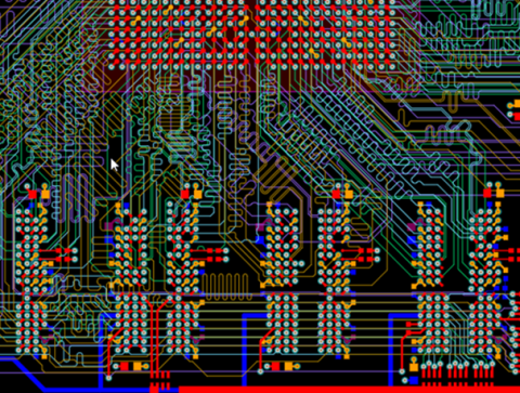
Copper splinters, or copper wear shorts, can occur in areas of the PCB where trace and pad clearances intersect. When designs are created on high-density multilayer PCBs with a large number of vias and crowded traces, the probability of copper splinters becomes greater. Etched copper in these areas leaves clearances between traces and pads, which become extremely small, and small copper splinters can cause a short circuit between these copper conductors.
The other potential cause of bridging is debris that separates from the board during etching without dissolving. After the debris falls into the chemical bath, pieces of copper can float and then land on another board before fully dissolving. In some instances, undissolved copper exposes copper plating normally covered by a solder mask and sets the stage for corrosion. In either type of copper splinter scenario, your design tools need to allow you to define strict clearances between pads, traces, and vias.
Prevent Copper Conductor Bridging Mistakes in Circuits
As a result, you need to establish design rules and electrical rules that define trace widths and clearances between copper in different parts of a circuit. The design rules engine in Altium Designer allows you to set specific clearances in your PCB layout to prevent worst-case hairline shorts due to copper bridging during etching.
- There are some common DFM errors that can lead to short circuits or accidental solder bridging during assembly.
- Poor quality manufacturing processes or materials can produce hairline short circuits between a copper conductor and a plane, pad, or solder point.
Learn more about hairline short circuits in your circuit board.
- Low-quality design software might allow you to route a dense board in a way that causes a short circuit.
See how to route a dense board in Altium Designer without causing short circuits.

Polygon copper pour becomes part of a net as long as it is not left floating. Your copper pour needs to be carefully placed so as not to bridge power and ground, causing a short circuit.
Unified Design Tools Help Catch Layout Errors and Short Circuits
Your design tools play an important role in ensuring your next PCB can make it through the production line without short circuits or other errors. In addition to rules-checking features and a set of CAD tools for circuit board layout, you need to generate a complete set of fabrication documents for your PCB. When all your PCB design features are available in a single application, everything you need for successful design and fabrication can be found in a single application.
Error-free Design and Fabrication in Altium Designer
The layout and routing tools in Altium Designer are built on top of the same design rule engine, which ensures your board does not contain critical design errors that cause short circuits. By checking your circuit board design against design rules as you create your layout, you’ll catch errors early and ensure high yield during manufacturing. Make sure your next design and production run are successful with Altium Designer.
- Altium Designer creates a rules-driven design interface with a complete set of design, layout, and routing features. The online rules-checking engine searches for design errors as you create your circuit board, including short circuits in every copper conductor.
Learn more about the rules-driven PCB design tools in Altium Designer.
- Every design and layout feature you need can be found in Altium Designer, and all in a single program.
Learn more about the complete set of design and layout features in Altium Designer.
- PCB design in 3D lets you spot design errors before you prepare your board for manufacturing and assembly. You can spot collisions between components and correct placement errors.
Learn more about ECAD/MCAD co-design in 2D and 3D in Altium Designer.

You can create polygons and spot copper short circuits in 3D with layer view utilities and MCAD features in Altium Designer
Simple routing errors cost companies loads of money, but a set of integrated PCB design tools can help you spot short circuits and prevent copper wear short circuits. Altium Designer creates the world’s most powerful rules-driven design environment. There’s no better way to achieve this copper confidence than with strong design software like Altium Designer.
Altium Designer on Altium 365 delivers an unprecedented amount of integration to the electronics industry until now relegated to the world of software development, allowing designers to work from home and reach unprecedented levels of efficiency.
We have only scratched the surface of what is possible to do with Altium Designer on Altium 365. You can check the product page for a more in-depth feature description or one of the On-Demand Webinars.

关于作者
Related Technical Documentation
相关资源
目录
从设计到发布,全程无阻碍
- 让评审始终关联到正确的版本
- 减少交接中的混乱和返工
- 更早发现采购与发布风险
- 可独立工作,按需共享
开始使用
Thank you, you are now subscribed to updates.


 沪公网安备 31010502006411号