

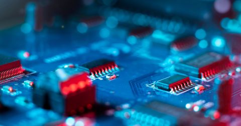


High Speed Routing Guidelines for Advanced PCBs


You can create this advanced board with these high speed routing guidelines for advanced PCBs
Newer designs are continuing to get faster, with PCIe 5.0 reaching 32 Gb/s, and PAM4 pushing signal integrity and speeds to the limit. Proper interconnect design must account for the lower noise margins of advanced devices, impeccable power stability requirements, and much more to ensure signals can be received properly.
With advanced devices running at lower signal levels, high speed routing guidelines are focused on preventing signal loss, distortion, and reflections from impedance discontinuities throughout interconnects. With ultrafast signaling, particularly with the use of multilevel signaling, you’ll need to seriously consider all the high speed design guidelines presented here and start to put them into practice.
Important High Speed Routing Guidelines
With high speeds reaching well into the sub-nanosecond regime, particularly in newer PCIe generations, and to support high speed networking equipment, any designer should keep some basic high speed PCB routing guidelines in mind. With newer devices continuing to break the speed limit, you’ll most likely need to keep all of these guidelines in mind, rather than picking a few to satisfy your application.
Stackup for Controlled Impedance Routing and Power Integrity
Your stackup is as important for signal integrity as it is for power integrity. Similarly, as signal bandwidths extend further into the 10’s of GHz, particularly with multilevel signaling schemes (take PAM4 for 400G networking as an example), you’ll need to control the impedance of your interconnects to ensure proper termination and matching. You’ll also need to properly size your trace to try to minimize ringing (i.e., critically damp the transient response) while keeping impedance constant. This requires meticulous stackup engineering and interconnect design.
Differential Pair Routing and Length Matching
With common mode noise being a major problem in signal integrity, you’ll need to ensure sufficient coupling throughout the length of differential pairs as part of controlled impedance routing. This also requires phase matching along the length of a differential pair. The coupled region should extend directly to the receiver, where possible, while any uncoupled region should be length matched and confined to the driver in your interconnect. This ensures any common mode noise will be seen as being perfectly in phase and thus fully suppressed at the receiver.
Choose the Right Substrate Material
With faster rise times comes the need to find substrate materials with lower loss tangent and flat dispersion. Dispersion is very important here as it creates a continuous change in the impedance and propagation constant along the length of an interconnect. First, dispersion causes electromagnetic pulses (i.e., digital signals) to spread as they propagate. Second, the impedance seen at the rising edge of the signal will not match that seen at the falling edge of the signal in the presence of strong dispersion, leading to strong distortion. You should make sure the dielectric constant is flat with the relevant bandwidth, which easily spans 30 GHz in PAM4 at 12 Gbps.
Short Traces and Backdrilling
Traces should be routed as short as possible so that power losses are minimized. In the case where dispersion is a problem, this helps to minimize pulse distortion, as pulses will stretch due to dispersion. Vias should also be minimized on traces as they can create an impedance discontinuity if not designed to exacting impedance. Any vias present on an interconnect should be backdrilled, as any remaining via stub represents another impedance discontinuity, thus they present another opportunity for signal reflection. These stubs can also resonate at high speeds/frequencies, meaning they will act as antennas that couple noise into nearby interconnects.

Variation in microstrip characteristic impedance with frequency. Thanks goes to Yuriy Shlepnev from Simberian for producing this figure.
High Speed vs. High Data Rate: Multilevel signaling and Fiber
With simple OOK or NRZ-modulated signals, you effectively have two signal levels that define your binary ON/OFF states. In effect, your data rate is limited by the rise/fall time of signals as supplied by the driver on a differential interconnect. The move to higher data rates has pushed rise and fall times to the limit, ultimately reaching down to picosecond levels at 32, 56, and 112 Gbps.
This also pushes jitter allowances to extremely low levels, which requires sufficient power stability to ensure power bus ripple does not propagate to the output from an IC with high power draw. It is common to see ~1 ps/mV jitter being induced in driven ICs due to ripple on a PDN. This is where your PDN impedance needs to reach milliOhm levels or less in order to decrease the ripple on a PDN to as low as ~2% for 1.2 V devices, equating to a ~30 mV peak-to-peak voltage fluctuation. You’ll need to bring jitter down to the ~1 ps level or less, which becomes appropriate for PCBs that use multilevel signaling.
At such low signal levels, increasing data rate requires working with higher bandwidth density by routing more channels in parallel. In networking equipment, this will continue using differential signaling to interface with more parallel Tx and Rx multiplexed channels in ultrafast fiber optic networking equipment. Optics are being mounted directly onto the PCB and interfacing with system chips using fast photodiodes and higher bandwidth VCSELs.

Board-mount optical assembly for interfacing with a system controller on a backplane.
How can designers continue pushing data rates higher to meet demands in newer networking equipment and other advanced applications? In case you can’t see where this is going, we’ll start to see a convergence between optics and electronics at the PCB level that will ultimately reach the IC level. The major IC manufacturers are already coming together to develop a supply chain for silicon photonic ICs and to develop some level of standardization for these new products. This will help alleviate many of the signal integrity challenges and relax some design constraints for the PCB community, but it will also force designers to rethink the way they create advanced products.
The comprehensive set of routing tools in Altium Designer® is ideal for defining and implementing the high speed PCB routing guidelines presented here, and much more. You can define your important high speed routing guidelines as design rules and examine signal integrity with powerful simulation tools. These tools are integrated into a single platform, allowing them to be quickly incorporated into your workflow.
Contact us or download a free trial if you’re interested in learning more about Altium Designer. You’ll have access to the industry’s best layout, simulation, and data management tools in a single program. Talk to an Altium expert today to learn more.
Start the journey to switch over to Altium Designer today.

关于作者
相关资源
目录
从设计到发布,全程无阻碍
- 让评审始终关联到正确的版本
- 减少交接中的混乱和返工
- 更早发现采购与发布风险
- 可独立工作,按需共享
开始使用
Thank you, you are now subscribed to updates.


 沪公网安备 31010502006411号