


Better PCB Routing - How Altium Highlight Nets


Regardless of how many PCBs I design, I always find myself having to regularly review network paths on the schematics layer and Altium highlight trace routes on PCBs. The complexity reminds me of a maze where only one path is the right one for a particular network. All the connections must be accurate as errors made here will come back to haunt you later in the form of redesigns.
The best way to ensure network accuracy is by isolating it so that each connection can be visually verified and edited, if necessary. Without a robust software design tool, creating and editing schematic and PCB footprint data can be quite difficult and time-consuming. On the other hand, with the right PCB design software, functionality and capabilities the design process can be greatly simplified and the time required to generate design files significantly reduced.
Altium Designer® is a robust unified design environment for creating schematics and PCBs. This software package is designed to simplify functional data-heavy tasks so the primary part of the process is the creative aspect, which lies with each designer. One of the capabilities that facilitate this for the designer is the ability to isolate and evaluate individual networks for accuracy. Altium schematic Highlight nets will help you simplify your PCB design. In Altium Designer, multiple options enable you to leverage this capability to simplify the verification of connections and circuit paths and make sure that the design you send to your manufacturer accurately reflects the printed circuit board you need to build.
Highlighting Nets to Simplify Schematic Design
Although the schematic does not provide the layout that will be present on your manufactured board, it must be accurate and complete. In all but very limited cases, such as when you are adding an extra pad or part to a previous design or if the layout is quite simple, your PCB design will usually begin with the creation of a new schematic. Here you can define all of your components and create your nets, as shown in the schematic below.
Schematic example without highlighted nets
The connections in the schematic are all readily visible upon normal viewing, but the situation is rather complicated and the connections between the buffer and decoders are difficult to trace due to overlap among schematic nets. Altium Designer includes a feature that allows you to view, select, or zoom into a specific net in the schematic. Selecting or highlighting a schematic net allows you to keep the entire net within the enlarged view.
To pick out specific nets, bring up the Navigator panel while you have the schematic open. If you click on the “Interactive Routing” button (outlined in a red box in the image below) at the top of the panel, you will see the cursor change, allowing you to select a specific connection in your schematic. As soon as you click on one of the wires, the entire wire will be selected and the remaining portions of the schematic will become semi-transparent. This will also zoom into the portion of the schematic that contains the net such that it fills up the entire window.
Altium Schematic example with a highlighted net
In another case, you may know the name of the net you want to examine, but you are not sure where exactly it appears in the schematic. In this case, you can find the specific net in your schematic by browsing through the “Net/Bus” list in the Navigator panel. When you click on one of the nets in the list, it will highlight in the same way as shown above.
Finally, suppose you want to automatically select all wires in a net PCB schematic. In this case, you’ll want to use the “Net/Bus” list in the Navigator panel. Right-click somewhere in the “Net/Bus” list, and you will see a dropdown menu with a “Select Objects” option. Once you enable this, you can click through the list of nets, and all connections involving this net will be automatically selected. This allows you to modify or delete an entire net in your schematic without tracing along each portion of the net and selecting portions individually.
Altium Schematic example with a selected net
Note that this feature is very useful if you come across a design that was repeatedly updated and became overly complex. When you begin your design, you can avoid this type of complication involving multiple crossed wires in a schematic when you create your design using hierarchical schematics. This allows you to define connections between schematics and avoid the type of confusion shown above. However, you can always access this net-highlighting feature to highlight, select, or simply zoom into individual schematic nets.
Highlight Nets in the PCB Editor
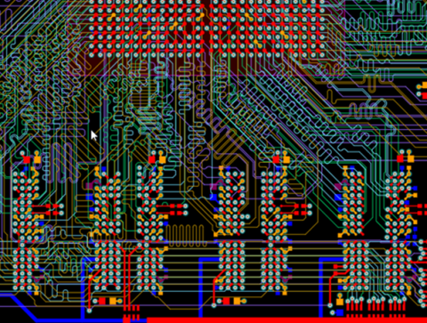
Today, most PCBs are comprised of densely packed components in a small area. More often than not, these boards contain SMDs and multiple signal layers, as shown in the example below. It is virtually impossible to accurately follow any Altium highlight trace for this layout without help. Fortunately, the Altium Designer highlighter provides help in the form of the ability to highlight nets, even when they extend to multiple layers.
As an example, let’s take a look at the MiniPC - SODIMM project in the Examples folder, which is provided in your library when you install Altium Designer. If you open this project and open up the PcbDoc file, you’ll see a complex layout for a computer memory module. The image below shows this board with all the layers enabled and visible. If you want to toggle which layers are visible, you can click on the “LS” tab at the bottom left of the PCB Editor window to open the View Configuration dialog.
PCB example with all layers visible and without highlighted nets
To highlight specific nets, click on the Panels tab at the bottom right of the PCB Editor, and open the PCB panel. This panel will list all Altium highlight net schematic classes and the nets contained in each class. The image below shows the SODIMM board with the negative end of the CLK net class highlighted; this net is named CL0_N.
PCB example with the CLK net class and CL0_N net highlighted
This panel also allows you to zoom into the selected signal net if you like, and you can toggle the zoom functionality at the top of the PCB panel. Note that this option is turned off in the above image. You can also change the colors of each portion of the board and the color of the highlighted net in the view configuration manager. Scroll down to the bottom of the View Configuration manager and expand the System Colors menu. This allows you to modify the color scheme in the PCB Editor, as well as the color of a selected/highlighted net. An example is shown below, where the CL0_N net is colored purple.
Modifying the color of highlighted nets in the View Configuration manager
A Third Option: Board Insight Display
Instead of going through the Panels tab, you have the option to highlight nets by simply hovering over them. This option can be set using the Board Insight Display, which can be accessed from the Preferences menu under the PCB Editor options. With this option set, you can quickly go from net to net verifying connections by simply moving the mouse.
Ensuring that your printed circuit board design, schematic, and board layout is connected correctly is critical to the successful fabrication and assembly of your PCB project layout. Sending your design out with incorrectly routed or misconnected nets is detrimental to your product development. Extended turnaround time and extra cost are but two of the penalties that you could face. These can be avoided by utilizing the ability to highlight nets.
Altium Designer is a robust software package with advanced capabilities, and creating schematics and PCBs can be simple and easy. The program’s unified design environment and extensive functionality provide you with many tools to simplify your design experience and pad you from design issues. For example, the PDNA package allows you to examine power integrity throughout your signal nets and power/ground planes during design. If changes are required, they can easily be applied to both your schematic and PCB. Highlighting nets in your schematic and PCB helps you make design changes quickly and easily.
For more information on how Altium highlight nets for your schematic and PCB design, contact an Altium Designer PCB design expert.

关于作者
Related Technical Documentation
相关资源
目录
从设计到发布,全程无阻碍
- 让评审始终关联到正确的版本
- 减少交接中的混乱和返工
- 更早发现采购与发布风险
- 可独立工作,按需共享
开始使用
Thank you, you are now subscribed to updates.


 沪公网安备 31010502006411号