


How to Optimize Your PCB Prototype for Production

At a Glance
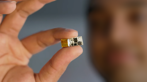
It’s often the case that PCB prototypes look nothing like a final product. If you’re transitioning from PCB prototype to volume production, learn more about optimizing your design.


If your startup is building the next great electronic product that will massively disrupt your industry, there is a long development process that eventually culminates in volume production. The transition to volume production often requires multiple prototype spins and development iterations, and it ends with a final round of design optimization before submitting a data package to a manufacturer.
In this article, I’ll detail some simple steps that help control costs and form factor when transitioning a prototype into a volume production environment. In other posts on the blog, you have likely seen an article on building a prototype PCB for your new product. This final design optimization before production will undo some of those steps and give you a finished design that is ready for volume manufacturing.
From Prototype PCB to Production
Run Through Your Remaining ECOs
Before doing any design optimization, run through your list of outstanding ECOs. If you’re at the point of optimization, the remaining ECOs should be miscellaneous items that do not affect the product’s core functionality. The remaining ECOs should also not increase EMI from the product as this might require another round of EMC testing and qualification. Implement any of these final changes in the schematics and the PCB layout, then proceed with finalizing the design for production.
Fabrication Features and Materials
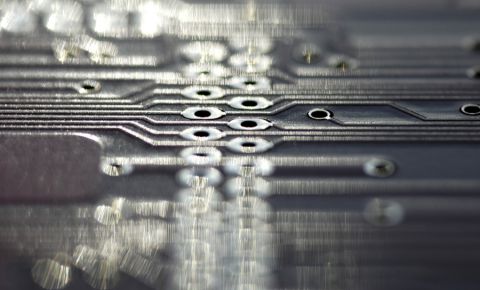
This step of design optimization has to do with both DFM and cost reduction. Smaller and finer fabrication features will increase the cost per board, as well as the potential for defects and number of scrap boards. One simple way to reduce cost per board is to enforce larger and consistent fabrication features.
- Select drill diameter sizes that put you in your target cost tier. If small vias aren’t required, then you can reduce costs by making your vias larger.
- Evaluate your plating needs; if you can get away with less expensive plating, then you should include this in your fabrication notes.
- If you don’t have via-in-pad in your PCB layout, then don’t fill and cap vias.
- If the materials being used in the design are overkill, then swap for less expensive materials compatible materials (you can use an IPC slash sheet to help with this)
Remove Excess Test Points and Solder Bridges
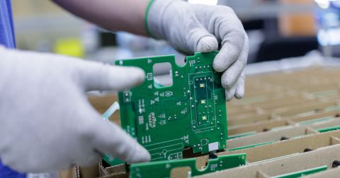
Prototypes will also typically contain a large number of test points that are used to probe or debug a PCBA during functional testing. Solderable bridges might also be present in the PCB layout. If these are not absolutely essential for continuity testing or in-circuit testing during assembly, or if they aren’t needed for the design’s operation in the field, then it’s recommended to remove these and their reference designators to free up board space.

Remove Excess Connectors, Headers, and Jumpers
In addition to copious test points, it’s common to break out any unused I/Os on components to pin headers. This allows the headers to be accessed during development for testing, or they can be used to interface with external boards or modules via flying leads. Jumpers on 2-pin headers are also commonly used in prototypes to provide configurability during testing and development.
If a connector, header, or jumper is not needed in the final product, then these should also be removed. Connectors can be some of the most costly elements in a PCBA, and they can take up a lot of space in an enclosure. Removing these reduces costs and board size, and it might allow you to fit an additional board into a panel.

Remove or Resize Reference Designators
Reference designators are generally included on a prototype as it aids inspection and debugging. For a production board, the reference designators may not be needed. Therefore, most of the designators could be removed, or they could be resized to reduce the space they occupy on the board. The caveat here is that reference designators should be included on the assembly layer in the PCB footprint so that a complete assembly drawing can be created; this will aid inspection on the assembly line.

Final BOM Cleaning
Finally, we come to an important point relating to front-end design: cleaning the BOM. This should be performed during schematic capture with three goals:
- Identify obsolete/out-of-stock/hard-to-source components and find alternatives
- Consolidate similar parts to the same part number
- Create a list of alternative parts for the assembly
Before finalizing a design, it’s important to do the first point again just to check for any unsourceable components and select alternatives. The second point is also important from a cost perspective as it could provide volume discounts when producing at high volume.
Check Your Manufacturing Data
Once all changes have been implemented, it’s time to generate your PCB design outputs in the required formats for your manufacturer. Make sure to update your fabrication and assembly drawings, regenerate fabrication files, and prepare these against the design data. Your manufacturer will also put the fabrication data through a review and compare copper connections in your Gerbers to your netlist.
In closing, heed these words of wisdom from Greg Papandrew, one of our recent podcast guests. In this conversation, he illustrates a situation where a small reduction in per-board costs translates into huge savings throughout a high volume production run.
Once you’re ready to prepare your design outputs and review your data, use the OutJob File feature and the world-class CAD tools in Altium Designer®. To implement collaboration in today’s cross-disciplinary environment, innovative companies are using the Altium 365™ platform to easily share design data and put projects into manufacturing.
We have only scratched the surface of what’s possible with Altium Designer on Altium 365. Start your free trial of Altium Designer + Altium 365 today.

关于作者
Related Technical Documentation
相关资源
目录
从设计到发布,全程无阻碍
- 让评审始终关联到正确的版本
- 减少交接中的混乱和返工
- 更早发现采购与发布风险
- 可独立工作,按需共享
开始使用
Thank you, you are now subscribed to updates.


 沪公网安备 31010502006411号