Thermal Relief Guidelines for PCB Layout

At a Glance
Sometimes, thermal reliefs are a DFA measure for a new PCB. Here’s when you should use thermal pads in a PCB.


Whenever you create a footprint in a PCB library, one of the things that you don't automatically assign in the footprint is the presence of a thermal pad (thermal relief). Instead, this is applied in the PCB layout, sometimes with a design rule or with an automated tool. A blanket design rule applied to all components can cause the application of a thermal relief where it may not be necessary. For example, plane or large pour connections on through-hole components can have different demands than SMD components going through reflow. Because the demands are different, when should you use relief on thermal pads?
In this article, I will give some guidelines on when thermal pads are most likely to be needed, and some instances where they do not provide any benefit. As we will see, the application of thermal pads on SMD parts or through-hole components depends on the PCB assembly process, acceptable yield, and component type or packaging.
Basics of Thermal Pad Usage
Thermal pads in a PCB layout are placed with the intention of preventing soldering defects during PCB assembly. Soldering defects can normally be reworked, but every rework cycle reduces the overall reliability of the PCBA and requires additional assembly steps that can accrue costs. Therefore, judicious placement of thermal pads may be helpful for preventing defects when scaling to high volume.
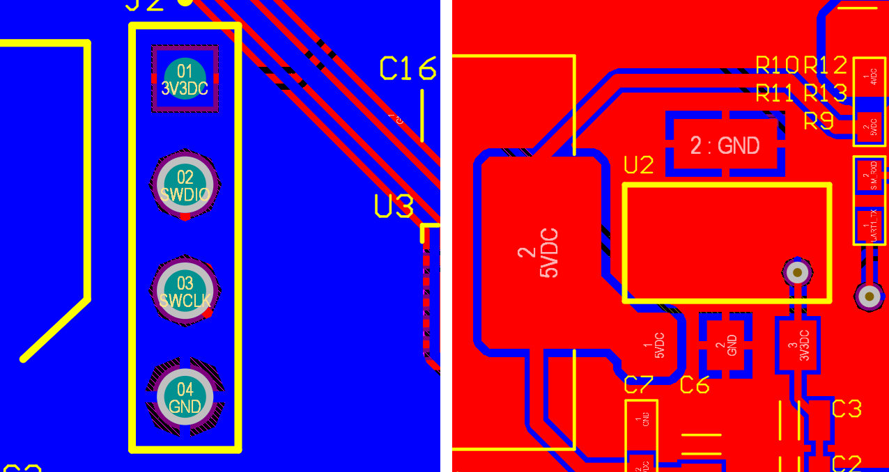
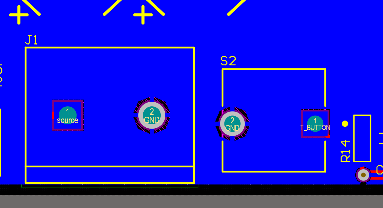
Two thermal pad examples on a through-hole part (left) and an SMD package (right) are shown below. These thermal pads do not need to be applied manually, they can be applied using a design rule and are normally applied on large polygons or planes.
The reason we place thermal pads is to prevent assembly defects during reflow or through-hole soldering, such as:
- Shifting of SMD components
- Tombstoning of SMD components
- Incomplete melting or solder balling during reflow
- Cold joints on through-hole or SMD parts
The basic idea is that the thermal pad controls a temperature difference across a pin or between pads on an SMD component. In reflow, shifting or tombstoning of parts is prevented when wetting occurs on all pads simultaneously. In through-hole soldering, such as hand soldering, wave soldering, or selective soldering, a stronger solder joint forms if heat cannot escape a pin into a large copper region, such as a copper plane.
Since thermal reliefs are applied via a design rule, what should be the scope of that design rule so that the reliefs are applied where they are needed most? We can look at this from two perspectives: SMD pads and through-hole pins.
Thermal Reliefs on Through-Hole Pins
As was mentioned above, the most important location to place a thermal relief for a through-hole pin is on the connection between the pin and an internal plane. The thermal pad only needs to be applied on the layers with plane connections; if there is a trace connection on the same pin in a different layer then another thermal relief is not needed on the trace layer. This is applied with a plane connect rule in your PCB design rules editor.
Some designers, including myself, will use copper pour to define a plane rather than place a plane layer in the PCB stackup. So the question becomes, do you also need the relief applied on large copper polygons?
If the polygon is being used as a plane, then they are equivalent layers of copper and the thermal pad should be applied. If the copper pour is smaller, then sometimes it is a judgment call. For example, large power rails can be drawn out as copper polygons, but these polygons do not necessarily need to have a thermal relief applied on the polygon connection. Personally, I prefer to look at these on a case-by-case basis: the more a copper pour region looks like a plane layer, the more likely I am to add a thermal relief to the through-hole pin connection.
Thermal Reliefs on SMD Pads
This is also a bit contentious and somewhat confusing due to default application of design rules. If your thermal pad rule applies reliefs everywhere, then this will also apply on all SMD pads, including pads that connect to polygons or copper fills. So of course, the question is, should you apply these reliefs on SMD pads when there is a copper pour or plane connection?
SMD parts will go through reflow soldering when producing at scale. This requires the entire assembly to soak up to a high temperature, which in theory will eliminate any temperature difference across the pads on SMD parts. This would mean that, in general, we don't need to have thermal relief connections on SMD components.
Of course, reality can be very different, as I discovered in a recent OnTrack podcast episode with Chrys Shea. Take a look at the video clip below, where Chrys describes some instances where one is more likely to observe a tombstone or shifting defect during reflow soldering, especially on very small SMD packages.
So should you use thermal relief connections on SMD parts? I think the answer is very often “no.” On integrated circuits, they certainly are not necessary or desirable. On SMD passives, the likelihood of needing them increases as the case size is smaller, and they may be needed due to the reflow issue described above.
Whether you need to build reliable power electronics or advanced digital systems, use the complete set of PCB design features and world-class CAD tools in Altium Designer®. To implement collaboration in today’s cross-disciplinary environment, innovative companies are using the Altium 365™ platform to easily share design data and put projects into manufacturing.
We have only scratched the surface of what’s possible with Altium Designer on Altium 365. Start your free trial of Altium Designer + Altium 365 today.

关于作者
Related Technical Documentation

相关资源


Thank you, you are now subscribed to updates.


 沪公网安备 31010502006411号