


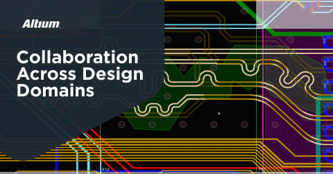


Integrated Electronics Manufacturing and Design Collaboration

At a Glance
Improve manufacturability and avoid redesigns with integrated electronics manufacturing and design collaboration. Learn how to streamline production.


Advanced devices require collaboration among multiple team members to ensure functionality and manufacturability. With embedded systems, this extends beyond a hardware team to include software developers. If you want your new product to be manufacturable at scale, then at some point, you will need to involve your manufacturer in the collaborative process. This is especially true with high speed digital devices and high speed analog devices.
If you consider the factors in these advanced systems that affect performance, most of them boil down to two important design aspects: layout and materials. The layout choices you make will affect device functionality by influencing losses, crosstalk, EMI/EMC, and other aspects of signal integrity/power integrity. The same goes for the materials you choose in your stackup. If you can collaborate with your fabricator early in the design process, you can overcome problems in all of these areas and avoid costly redesigns before production.
So what is the best way to collaborate with your manufacturer? This is where you need an integrated electronics manufacturing and design system that allows information to be passed between all parties. This goes far beyond emailing specifications and design changes between your designers and your manufacturer. Instead, you need a system that allows a designer and manufacturer to push design updates to each other in real time.
Designers Need to Work With Manufacturers Early
Manufacturers will tell you in no uncertain terms: designers need to talk to fabricators early in the design process. Furthermore, a more advanced design requires earlier fabrication. If you approach your fabricator after you complete your layout, you may find that one of your layout decisions for overcoming a power integrity or signal integrity issue is completely unbuildable. Unless you want your new design to remain in digital form, you'll be forced to go back and redesign unbuildable portions of your design, possibly rewinding back to the beginning of the design process. This often leads to compromises in functionality, electrical performance, and/or reliability. Here are some basic points to check with your manufacturer before you create your layout:
Board and Interconnect Architecture
Some designers will be fine working with the traditional trace-and-via interconnect structure. They may not be working in the HDI regime or using standard FR4 substrates. Other design teams need to work on the cutting edge, which requires advanced materials, unique layer transition structures, rigid-flex or fully-flex substrates, or unconventional RF structures. You'll find plenty of these design decisions in the HDI and microwave/mmWave worlds.
Your manufacturer should be able to give you some advice on the range of structures that they can reliably fabricate. Something as simple as picking up the phone or sending an email to ask about the manufacturability of proposed designs goes a long way toward preventing a redesign and ensuring higher yield. Taking some time to learn about your fabricator's processes can also help you determine whether certain designs will be manufacturable with a high yield. This is especially important with unique layer transition structures (such as ELIC, VeCS, VIPPO, and landless vias), interconnect designs (such as GCPW and SIW), and embedded shielding structures.
Laminate Stocks
While it might sound obvious, checking laminate stocks before design is also critical. You can build a product with the desired electrical performance. Although there are IPC standards that aim to define laminate compatibility requirements, these are more process-focused and not electrically performance-focused. If you've qualified a particular material electrically, mechanically, and thermally, you may be forced to switch to a non-qualified laminate material once you submit the board for quote.
A simple email to the manufacturer is enough to get the process started. If they need to see your design data or your manufacturing outputs, you can share the design information with them, and they will be able to tell you whether they can supply the laminates you're requesting.
Can They Build Your PCB Stackup?
If you're foregoing the standard stackup route and instead you're taking the lead role in designing the PCB stackup with specific materials, the stackup still needs to be qualified to ensure it can be processed successfully. Complex multilayer stackups with multiple sub-laminations, exotic materials, via transitions, backdrills, and copper weights will require significant processing work that demands your fabrication house review the stackup before you work through the design.
Consider the PCB below, which contains a BGA with a dog bone fanout. It looks pretty standard, and due to the ball pitch, it probably uses simple through-hole vias and does not require extremely thin laminates for blind vias to complete the escape routing.

Of course, we can't say anything about the build requirements for a PCB stackup just by looking at the top layer!
What if this PCB was part of a more exotic stackup? For example, what if the PCB had a very high-frequency RF section, boomerang vias, press-fit pins with specific layer spans, or other common build options? The stackup might end up having any of the following characteristics:
- Sub-laminations with deep, mechanically drilled buried vias
- Backdrills only in a single sub-lamination
- Hybrid RF stackup design
- Hybrid HDI design (e.g., blind vias in one layer)
- Non-symmetric stackup thickness
- Non-standard copper weight
A PCB fabricator will need to review all aspects of these stackups in order to ensure the build is even feasible. In many cases, the fabricator can recommend simple changes that increase the yield and reliability of the build without impacting electrical functionality.
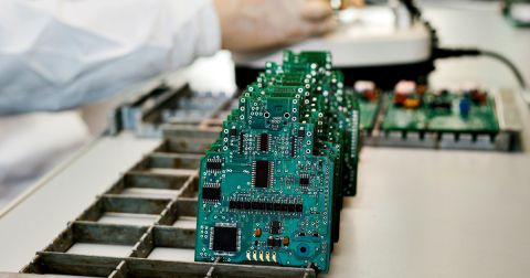
Assembly
This is one of those areas that can be taken for granted, especially when everyone focuses on DFM. If you are using a separate assembler, there are some aspects of assembly, such as soldering to die-attached paddles with thermal vias, that assemblers can reasonably accommodate. However, some fabricators will give the same board no-bid status. It can be difficult to work out these disagreements, but collaboration through an integrated electronics manufacturing platform will allow you and your manufacturer to find a balance.
Required Documentation
Most manufacturers will list this on their website, but it never hurts to ask which design file formats, BOM formats, or any other information your manufacturer will need to reliably build your board. If you're looking to have a unique board architecture produced, it's best to err on the side of caution and provide more information than you would for a standard PCB. In general, you'll need to provide the following list of deliverables to your manufacturer:
- Gerber files (RS-274-D, RS-274-X, or X2)
- Fabrication and assembly drawings, including a stackup diagram
- Drill files and pick-and-place files
- Bill of materials
- Netlist in standard file formats
- And, of course, your schematics and PCB layout files
What Does Integrated Electronics Manufacturing Look Like?
When your designers and manufacturer work together with an integrated electronics manufacturing and design platform, a fabricator and designer can collaborate on any required design changes early in the design process. Your manufacturer can suggest design changes and push them back to the designer. The designer can then evaluate these suggested changes and then choose to accept or reject them as needed. This is the type of environment you'll find in Altium 365.
In addition to collaborating on any required layout, material, or stackup changes, a designer and manufacturer can work to source components and determine possible replacements when needed. Your PCB design collaboration tools should also provide sourcing information so that you can spot components that are nearing the end of their life cycles and locate new components as needed. Up-front consultation and continuous collaboration go a long way toward eliminating time-consuming redesigns.

When you use the integrated electronics manufacturing and design capabilities in Altium 365, you and your manufacturer will be able to collaborate on complex design decisions in real time. You'll have access to a powerful data management system that integrates with the industry-standard PCB design tools in Altium Designer. Together, these two powerful tools provide a complete PCB design and production planning solution in a single platform. Start using Altium 365 today to take your product from idea to production effortlessly!

关于作者
Related Technical Documentation
相关资源
目录
从设计到发布,全程无阻碍
- 让评审始终关联到正确的版本
- 减少交接中的混乱和返工
- 更早发现采购与发布风险
- 可独立工作,按需共享
开始使用
Thank you, you are now subscribed to updates.


 沪公网安备 31010502006411号