


IoT PCB Design: It's More Than Just Hardware Development

At a Glance
Altium 365 makes IoT PCB design and coding easy. Share your designs, control revisions, and fork projects directly in Altium Designer or through Altium Concord Pro.


IoT products are lovely and sometimes frustrating products. Design teams need to be multifunctional to design these products successfully. They need to get the hardware, embedded software, web platform and/or app, and mechanical enclosure perfect if they want to see market success. Problems in any of these areas mean your new product will be substandard and, eventually, competitive products will win market share.
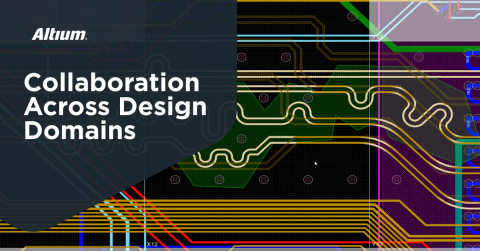
So what does it take to ensure these products are designed successfully? IoT PCB design isn’t just about the hardware. It’s also about user experience and form factor. This means any IoT PCB design team needs to work across disciplines, and everyone needs a view of each other’s deliverables. Cloud platforms and on-premises networking platforms help make this type of collaboration possible.
IoT PCB Design Teams are Multifunctional
If you’ve bought an IoT product recently, such as smart appliances or a home security system, you’ve probably had to download an app to your phone and create an account on the company’s website. These products can also have interesting enclosures that require exacting design specifications. These different aspects of an IoT product mean an IoT PCB design team needs to be multifunctional and need to collaborate for successful design. Your IoT design team will include people from the following disciplines:
- Electronics engineering. These folks need to design the schematic and ensure components chosen for the board are sourceable before handing a design off to the layout engineer and the software team.
- PCB layout engineering. This group is self-explanatory; they need to arrange components, route traces, ensure power/signal integrity, and all the other tasks that go into creating a great PCB layout.
- Software/mobile app engineering. The software team usually needs to wait until the electronics engineers finish the basic design, as this will determine which components they’ll be working with. If a web platform is involved, the web team can get started early, developing the basic web architecture, UI/UX, and API framework.
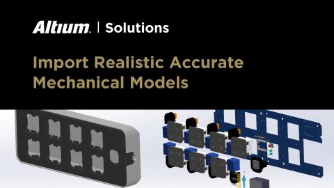
- Mechanical engineering. This group needs to work with the PCB layout engineers to ensure the product’s enclosure will fit the finished PCB and vice versa. For products that bend or fold, they also need to ensure any flex or rigid-flex boards will conform to the enclosure.
Recent IoT projects we’ve worked on required collaboration between myself (as lead engineer/manager), the PCB layout engineer, the embedded developer, the client’s mechanical designer, and the client’s software development team. These types of projects can get very complex when so many people are working on the same goal, and keeping everyone on the same page takes collaboration tools that can support all the different file types required to create a new platform.

How Multifunctional Hardware Teams Can Collaborate
Anyone that’s worked as part of a software team is probably familiar with Slack, Jira, and other collaboration and chat tools for sharing code, tracking task progress, and entering tickets for outstanding development issues. The collaboration tools you use should enable some important tasks as part of IoT PCB design and development:
- Supply chain visibility. Anyone that’s designed a schematic around some specialty components, only to find their desired components have gone obsolete or have months-long lead times, know the importance of supply chain visibility. Design teams need to start sourcing components early to reduce their risk of redesigns later.
- Commenting, project release control, version control, and forking. These features are exactly what you’d find in a GitHub-style architecture for hardware design. It shouldn’t be limited to code commits, PCB layout and mechanical drawing commits need to be accessed as well.
- User access control. Not everyone in your organization will be working on the same set of tasks. A system with user access control (both for viewing and editing) ensures the right people can access projects on an as-needed basis.
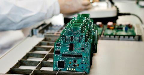
- Sharing fabrication data. IoT PCB design teams will eventually need to work with a manufacturer to get a board produced. Bringing a manufacturer into a collaborative process is a huge value add that can reduce turn times and help you spot DFM errors early.

As more companies go remote, even in the realm of hardware development, design teams will need cloud-based or on-premises systems that integrate with their design software. The current class of remote collaboration tools can’t provide the accessibility needed to instantly import design data into ECAD and MCAD programs while also providing version control, component management, and user access control. It’s time for hardware teams to use a new platform that unifies PCB designers with mechanical designers and, soon enough, embedded developers.
Altium 365 is the only platform that integrates Altium Designer with apps like Altium Concord Pro and the Altium Viewer, making collaboration easy for multifunctional teams. Engineers from all disciplines can see each other’s design data and instantly import it into Altium Designer or view it through an Altium Concord Pro web instance. The version control, commenting, and access control features let your team create a GitHub-style platform for hardware development. This is an ideal way for IoT PCB design teams to collaborate on complex projects.
Altium Concord Pro on Altium 365 is bringing an unprecedented amount of integration to the electronics industry until now relegated to the world of software development, allowing designers to work from home and reach unprecedented levels of efficiency.
We have only scratched the surface of what is possible to do with Altium Concord Pro on Altium 365. You can check the product page for a more in-depth feature description or one of the On-Demand Webinars.

关于作者
Related Technical Documentation
相关资源
从设计到发布,全程无阻碍
- 让评审始终关联到正确的版本
- 减少交接中的混乱和返工
- 更早发现采购与发布风险
- 可独立工作,按需共享
开始使用
Thank you, you are now subscribed to updates.


 沪公网安备 31010502006411号