


Making a PCB with a 3D Printer Still Requires Design Expertise


Designing PCBs for 3D printing can follow one of two routes: additive or subtractive manufacturing. Your PCB design software should be adaptable to either technique and should have the capability to generate the files required for your 3D printer to accurately lay etch or deposit your traces. Working in Altium Designer’s unified design environment integrates your design tools in a single interface. Altium Designer offers the only design package with tools that can adapt to any fabrication strategy.
ALTIUM DESIGNER
A PCB design software package with the best CAD tools that are adaptable to 3D printing.
3D printing is a convenient way to create just about anything the mind can imagine. You can create practically anything with a 3D modeling program and print it out within the comfort of your home, even with a desktop 3D printer. However, 3D printing electronics and circuit boards have remained somewhat out of reach, with only a number of companies and individuals manufacturing the required equipment. Even if you have the required equipment and conductive filament for making a PCB with a 3D printer, you are only halfway to your goal of 3D printing your own PCBs.
3D printing a PCB requires electronics design software that includes ultra-accurate CAD tools and 3D modeling tools. Your printed circuit board design software requires more than just the standard schematic and layout tools that come with other design software packages. You’ll need a design package that allows the PCB printer precise definition and visualization of each element on your PCB, including surface traces, components, and unique board shapes.
Additive versus Subtractive Manufacturing
Many circuit board printers on the market can be used to lay traces of conductive ink, and you’ll subsequently have to assemble your device by gluing components to the fragile circuit board. Your 3D printer needs a copy of your trace layout, and a conductive is deposited directly on the board.
Instead of using a subtractive fabrication method, you can create an inversion image of the conductive traces on your printed circuit board. You can then etch your conductive traces from a copperized glass fiber plate. Combining a diode laser with the CNC capabilities of a 3D printer allows you to selectively etch off unused copper. You can then solder SMT/SMD components to your board with a low-temperature solder.
Choosing the Right Fabrication Techniques
Using a 3D printer to fabricate your PCB is a great way to start building a functional prototype of a new device. Whether you are removing copper foil from your PCB by etching or removing a fine layer off a photosensitive board with laser and selectively exposing copper, you’ll need design software with accurate CAD tools to define your layout. Your PCB design software should also generate 2D or 3D CNC data for your printer directly from your layout. The best PCB software allows you to use either additive or subtractive techniques for fabrication.
- A number of 3D printing techniques can be used for prototyping and fabricating your PCBs.Learn more about using different 3D printing methods for PCB fabrication.
- 3D printing your PCBs brings several benefits, such as reduced costs, turnaround times, and standardized designs. Learn more about the benefits of in-house additive manufacturing.
- If subtractive manufacturing is not your preferred fabrication method, conductive inks can be used in additive PCB manufacturing. Learn more about using conductive inks for PCB fabrication.

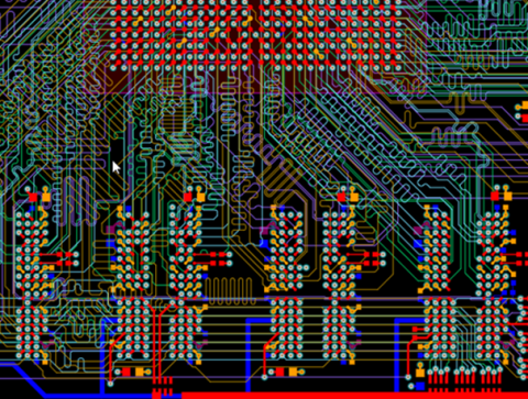
3D viewer in Altium Designer
Defining Design Rules for Your 3D Printed PCB
Routing traces in your PCB layout requires obeying a set of design rules that ensure your device will meet its functional requirements. Many 3D printers can etch traces as thin as 0.2 mm. Your layout software can save you a significant amount of time with your layout when you can define design rules in your PCBs. Your PCB design software package should give you the power to specify your trace width and should help you automatically route traces between components.
Newer 3D printing systems for printed circuit boards can also be used to fabricate multi-layer PCBs with a machine the size of a small office printer. If you are planning to fabricate multi-layer PCBs with a 3D printers, your design software needs to include an intuitive layer stackup manager that allows you to completely customize your layer arrangement.
Design Tools for Your 3D Printed PCB
Your circuit board trace routing tools should do more than just define trace sizes and automatically define traces between components. Your design tools should interface with your design rules and routing directives, allowing you to route accurate traces and design a layer stackup for any application. You should also be able to define the copper weight used in your circuit board traces and quickly translate this information into G-code, Gerber, or DXF files for your 3D printer.
- Excellent routing tools like part, pin, and differential pair swapping can greatly improve your productivity and ensure your designs can meet the capabilities of your 3D printer. See how interactive routing tools can improve your design workflow.
- Fabricating more advanced PCBs with a 3D printer requires the same multi-layer stackup manager you would use in a conventional PCB. Learn more about defining and editing your PCB layer stack.
- Designing PCBs for printing requires implementing DFM practices into your design workflow. Learn more about design for manufacturing.

Close-up 3D view in Altium Designer
Altium Designer Offers the Best ECAD Tools for 3D Printing
Other design packages separate your critical design tools into separate modules. Only Altium Designer integrates these tools into a single design environment, and these tools are adaptable to any fabrication method. Altium Designer is the only PCB design software package that has unified MCAD and ECAD design, making these design tools perfect for designing PCBs for 3D printing.
Altium Designer Has the Best 3D Design Features
The 3D design features in Altium Designer have set a new standard in the PCB design software industry. The unified design model in Altium Designer integrates your design tools into a single interface and allows you to use them for 3D ECAD design. Instead of using separate pieces of software for different design tasks, try working in the only PCB design software package that unifies your tools in a single interface.
- The unified data model in Altium Designer integrates your design features into a single package. Never again will you have to move between design programs just to finish simple design tasks. Learn more about the unified data model in Altium Designer.
- Altium Designer has fused ECAD and MCAD integration into a set of extraordinary 3D design tools. Learn more about ECAD/MCAD design integration in Altium Designer.
- Altium Designer’s 3D design tools are tailor-made for anyone that wants to 3D print their next PCB. Learn more about the single-layer 3D viewer in Altium Designer.
If working with separate programs is hampering your PCB design process, you need to work in a unified design environment. Altium Designer integrates your schematic design, routing, and rules-checking features into a single interface. The 3D viewing and design features make designing PCBs for 3D printing easy, allowing you to reduce your fabrication times from weeks to hours.
3D and additive printing are the future and may even replace the conventional PCB fabrication processes. A great PCB design software package like Altium Designer turns making a PCB with a 3D printer into a much easier process. Customize every aspect of your PCB design and generate the fabrication data required for your 3D printer. You’ll have access to the best design, routing, rules checking, and simulation tools, and all within a single design environment.

关于作者
Related Technical Documentation
相关资源
目录
从设计到发布,全程无阻碍
- 让评审始终关联到正确的版本
- 减少交接中的混乱和返工
- 更早发现采购与发布风险
- 可独立工作,按需共享
开始使用
Thank you, you are now subscribed to updates.


 沪公网安备 31010502006411号