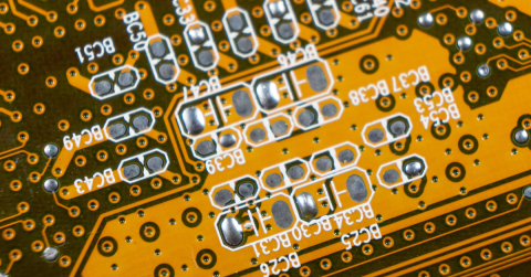
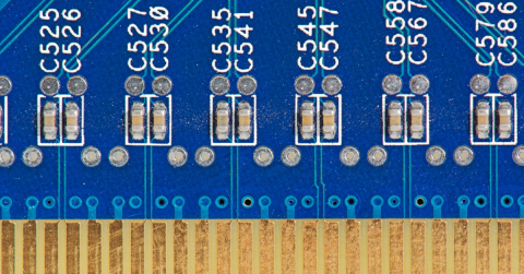
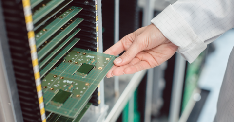
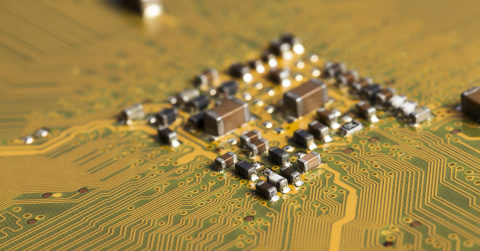
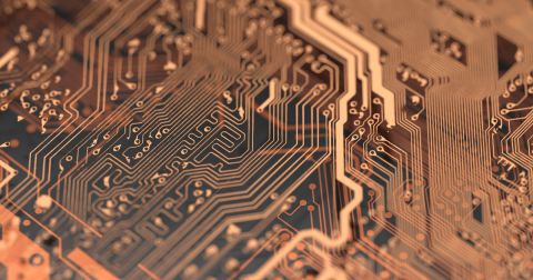

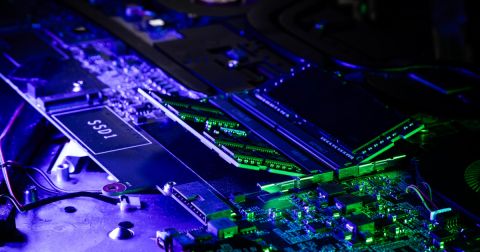
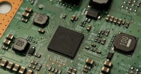

The traditional approach to circuit board design has been to place the components on the top and bottom surfaces of the board. This process is well supported by circuit board assembly houses, which typically use automated pick and place machines to position each component, ready to be soldered onto the surface. The ever increasing demand for smaller and more integrated electronic products,…
Related Videos Define New Layer Stacks Layer Stack Regions The PCB is designed and formed as a stack of layers. In the early days of printed circuit board (PCB) manufacturing, the board was simply an insulating core layer, clad with a thin layer of copper on one or both sides. Wiring was formed in the copper layer(s) as conductive traces, by etching away (removing) unwanted copper. A simple,…
How many of us got into electronics because we were drawn by the myriad of cool switches, knobs, lights and other suitably gadget-centric controls? Fast forward a good few years and that allure is still there, only it is now replaced with the "Snazzy GUI" factor - electronic products that have a sleek, sexy interface. Central to these ever-advancing (and shrinking) product interfaces is touch…
The Technology 目前用于制造印刷电子电路的技术包括: 激光直接成型 - 在需要制造精细导体结构时使用。 3d打印 - 成型 DuPont InMold - 将电路印刷到塑料基板上,然后将其热成型并注塑成最终产品形状。 双射成型 - 这是用于具有粗导体结构的大量生产的极好方法。 技术差异 就技术提供的内容而言,任务是一样的 - 将电子元件通过导电通路连接在一起,形成一个执行特定功能的电子电路。不同之处在于电路构建的方法。 从设计角度来看,传统的印刷电路板(PCB)被设计为一系列导电层,每个导电层通过绝缘层与其相邻的导电层隔开。导电信号通路定义在这些导电层上。每个信号都留下一个元件插脚,水平地蜿蜒穿过导电层。当信号路径被现有的信号通路阻挡时,或者当信号需要到达另一个导电层上的元件插脚时,信号会垂直向上或向下移动通过相邻的绝缘层到达另一个导电层…
When using a Standalone or Private Server license, you may need to reactivate/refresh that license to be able to access and use the wire bonding functionality. For a Standalone license, this is performed from the License Management view. For a Private Server license hosted in the Altium On-Prem Enterprise Server or Altium Infrastructure Server, this is performed from the Admin – Licenses page of…
开始使用