Overview of PCB/PCBA Reliability Testing and Failure Analysis

At a Glance
PCB reliability testing and failure analysis go together. Here’s what you need to know and how to get started.


Reliability testing and failure analysis of a PCB/PCBA go hand-in-hand; when designs are stressed to the limit, their failure modes need to be determined through thorough inspection and analysis. Some of these tests and potential causes of failure are handled by manufacturers as they might arise during bare board fabrication, while other potential problems with the PCBA should be addressed by a design team during prototyping and design qualification. High reliability designs, such as in areas like avionics and defense, can require extensive environmental testing and qualification to ensure they will function in the intended environment.
To get started on this topic, it’s important to understand the qualification aspects that will govern your bare board design and the PCBA. We’ll look at the various dimensions of PCB/PCBA reliability, as well as some of the standard failure analysis techniques used to identify potential design change requirements.
PCB Reliability Testing Standards Overview
Reliability testing broadly involves exposure of a PCB or finished PCBA to extreme environmental conditions (heat, corrosion, humidity, etc.), followed by performance tests to ensure the device can withstand those conditions. Within the discipline of reliability testing, there are many possible sources of stress on a PCB and the finished PCBA:
- Mechanical loading (static load, vibration, and shock testing under MIL-STD/IPC/SAE stadnards)
- Thermal or climate loading (heat flux, extreme temperature, thermal shock under IPC-TM-650 2.6.7 and MIL-STD-202G; thermal cycling under MIL-STD-883 Method 1011, IPC-9701A [6], and JEDEC JESD22-A106)
- Electrical loading (high power, derating verification, EMC, all in conformance with IPC/IEC/SAE standards) and UL conformance
- Chemical loading (corrosion or other chemical exposure to match deployment environment)
- Exposure to ionizing radiation (computed as total ionizing dose (TID))
- Exposure to dust, particles, and liquids
- Artificial aging tests for electronics assemblies (HALT, HASS, HATS, etc.)
What’s Involved in Reliability Testing?
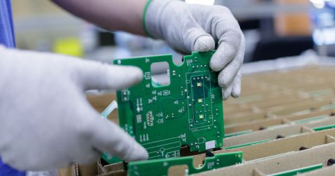
A PCB reliability assessment requires a set of tests that focus on each of the areas listed above. Basic fabricated board tests will be performed on your stackup by your fabricator, and they should be able to certify the bare board will conform to your requirements as you specify in your PCB fabrication notes. For the PCBA, testing and reliability can be more extensive. Your fabricator/assembler will perform their own series of tests and inspections to verify conformance to an IPC product class and basic IPC standards on bare boards, but it will often be up to the design team or a contract testing firm to run more specialized tests (environmental or chemical tests) on the design to verify reliability.
Guides to tests in any of these areas would involve a series of articles, so I won’t get into all of these aspects of reliability testing and verification. Standards documents provided by IPC, MIL-STD, SAE, NASA/DO, and other organizations provide guidance in this area, as well as specific procedures for performing these tests. IPC-TM-650 contains standardized test methods for PCBs, but the other documents mentioned above may go beyond the requirements in IPC-TM-650 for specific products and industries.
PCB Failure Analysis
Determining the limits of PCB reliability is all about pinpointing failures, as well as how they arise in the device. Once a board failure occurs, it needs to be investigated and Failure can arise gradually due to accumulated damage (e.g., fatigue), erratically (random or intermittent), or sudden (due to shocks). When failure modes are being investigated, application of the above tests involve cumulatively stressing the PCBA until failure (thermal, mechanical, and environmental), followed by examining the board to locate and examine the specific failure.
The table below matches the standard PCB failure modes to inspection and failure analysis methods used in a PCB.
|
|
|
|
|
|
|
|
|
|
|
|
|
|
|
|
|
|
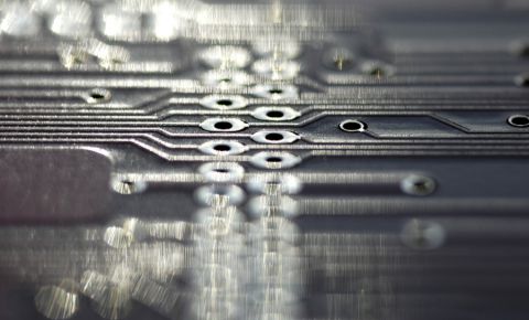
Identifying defects in each of these areas takes some skill. Some of these are obvious, such as extreme corrosion due to exposure to moisture, while others are only obvious to the trained eye. For example, identifying a failure from an X-ray image is not so obvious due to the contrast and resolution in the recorded image.

Something like conductive anodic filamentation due to prolonged operation at high voltage or fracture of a via barrel during operation is quite easy to spot, either from a microsection sample or from an SEM image. Both are clearly visible with the right imaging technique. As an example, the image below shows fracture clearly visible in a microsection, which may create an intermittent failure.

Once a defect or failure is identified, some steps should be made to prevent the problem from occurring during operation, or to modify the design so that it is more resilient against this type of problem. This has to be approached on a case-by-case basis, depending on the type of defect and mechanism that caused the failure.
Final Thoughts
The key to remember here is that no PCBA will be invincible, and any design can eventually be stressed until catastrophic failure. If the applied stresses are so extreme that they are highly unlikely to be ever encountered during operation when deployed in the product’s intended environment, then you can consider your design successful from a reliability perspective. When testing for reliability and investigating failures, it pays to consider the failure modes your device will be most likely to experience during operation and address those first.
Once you’ve used your PCB failure analysis results to identify required redesigns, you can implement design changes with the complete set of layout features in Altium Designer®. When you’ve finished your design, and you’re ready to release files to your manufacturer, the Altium 365™ platform makes it easy to collaborate and share your projects. Your manufacturer can also complete their own design review to help ensure high yield and quality as you scale.
We have only scratched the surface of what’s possible with Altium Designer on Altium 365. Start your free trial of Altium Designer + Altium 365 today.

关于作者
Related Technical Documentation

相关资源


Thank you, you are now subscribed to updates.


 沪公网安备 31010502006411号