


Ebook: Routing High-Density Interconnects with Reliable Microvias

At a Glance
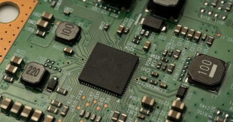
Routing high density PCBs is heavily rules driven and it requires understanding what contributes to microvia reliability.


As electronics have become miniaturized, the technologies used to route interconnects have been pushed to their limits, and new modes of designing PCBs with high reliability have become standard. HDI PCBs take a particular approach to routing interconnects through multiple layers to ensure reliability during fabrication, assembly, and operation. The critical structure that enables this is microvias, which are prone to failure if not designed properly. Some simple design decisions will have a major impact on reliability and solvability in an HDI PCB layout.
In this e-book, readers will receive an initial look at the reasons microvia reliability has come into the spotlight and why HDI PCB designers put reliability first when routing through microvias. Covered topics include:
- Warnings from the IPC regarding reliability of via structures in HDI PCBs
- How to design microvias to ensure reliability
- How to create a PCB stackup for a high density circuit board
- How to set up design rules for layout and routing in HDI PCB design
Click the PDF above to read more about routing in an HDI PCB layout and how to design interconnects for HDI PCBs. You can also read the original, full-length content here:
The IPC Warning About Microvia Reliability for High Performance Products
Everything You Need to Know About Microvias in Printed Circuit Design
Advanced High Density PCB Design in Altium Designer
How to Setup HDI PCB Layout and Routing in Your PCB Design Software

关于作者
Related Technical Documentation
相关资源
从设计到发布,全程无阻碍
- 让评审始终关联到正确的版本
- 减少交接中的混乱和返工
- 更早发现采购与发布风险
- 可独立工作,按需共享
开始使用
Thank you, you are now subscribed to updates.


 沪公网安备 31010502006411号