
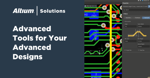


Using the Properties Panel for PCB Routing in Altium Designer

Routing is one of the most time-consuming stages of PCB design. Altium Designer has a large set of tools that allow you to do it as accurately and quickly as possible. This document will help you to learn how to manage your routing effectively and use it to its fullest extent.
The basis of PCB topology development in Altium Designer. By offering powerful routing tools, the system provides comprehensive settings. All groups of settings are arranged in accordance with the logic of the tool, as well as have context-dependent representation.

Properties panel overview
The properties panel automatically changes when a user activates the Interactive Trace feature to display the appropriate settings. The panel consists of several sections:

“Net information” section
Single-track routing
In the Net Information section for single-track routing, the following parameters are displayed:

Diff pair routing
For Diff Pair routing in the Net Information section a user can see the following parameters:

“Properties” section
Single-track routing

Diff pair routing

Multi-routing

Layer change
When you change layer, the Properties section will display detailed information about the configuration of the current via

“Interactive routing options” section


“Rules” section


关于作者
相关资源
相关的技术文档
Design to Release, Without the Friction
- Keep reviews tied to the right version
- Reduce handoff confusion and rework
- Spot sourcing and release risk earlier
- Work solo, share when needed
Get Started
Thank you, you are now subscribed to updates.
 沪公网安备 31010502006411号