


The Newest Advances in EDA: Modular Electronics Design


EDA has come a long way since the 1960’s. Image source: Autodesk
Before the birth of EDA, circuit boards and integrated circuits were all designed by hand or some other manual process. The need for more advancement in electronics design made clear the need for automation, a transition which took roughly 10 years and began with drafting in the mid-1970s. The publication of “Introduction to VLSI Systems” by Carver Mead and Lynn Conway in 1980 paved the way for chip design with programming languages that compiled to silicon. From there, EDA became a formidable industry which remains with us to this day.
Since 1981, the year of the birth of commercial EDA, there’ve been several innovations in this industry that have made it easier to build powerful electronics systems. With the continued growth of the semiconductor industry, the importance of EDA cannot be overemphasized. Since that time, we’ve seen innovation in EDA feature sets, as well as integration of existing feature sets into complete platforms. However, one can argue that there has been no radical innovation in the realm of EDA until only recently.
Innovation Challenges in the EDA Software Industry
Today’s EDA tools, when coupled with traditional PCB manufacturing processes, are in many ways responsible for limiting design freedom and limiting innovation. In the early days, electronics and circuit boards were something of an art form, and the layout was designed with fewer limitations or constraints. Engineers were free to design the way they wanted, and eye-catching circuits were beautifully laid out. Today’s EDA tools make it possible to automatically draw our circuits. Although the results may not be as artistic as circuits from decades past, it sure is more efficient, and we can pack more on an electronics board.
The course of innovation in the EDA industry has followed a similar path for a number of companies. It all started as schematic capture, followed by automated and semi-automated PCB routing, simulation capabilities, and 3D rendering. The UX across multiple tools has become roughly homogenized, depending on the level of integration. These innovations have spread across multiple platforms, but little innovation has happened since these critical features were incorporated into popular desktop applications.
The lack of innovation among EDA companies has created an interesting phenomenon in the industry. If you take a look at most EDA tools and platforms, you will observe something familiar with all of them. These platforms all basically do the same thing, and most have roughly the same interface. These platforms are primarily differentiated by the level of integration and compatibility with other design and data management tools they offer. To be fair, the most innovative EDA companies are expanding their capabilities into other areas like FPGA design, real-time MCAD collaboration, and more powerful simulations.
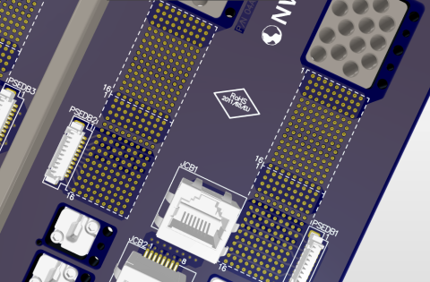
If you’re not an experienced PCB designer, then creating this type of layout can be very time-consuming
Even EDA platforms like Classic Upverter, which differentiates itself by providing a complete browser-based EDA and component management platform, is still in danger of falling into the same loop as desktop EDA applications. Placing these tools online and building a web-based version of desktop tools is a natural innovation in that it provides support for collaboration. Zak Homuth, the founder and CEO of Classic Upverter, has stated that the EDA industry is hostile to innovation in a recent article on Medium.
Modular Electronics Design Tools are Bringing Change
With design reuse becoming more important, EDA tools have allowed designers to package portions of a PCB into libraries, allowing designers to layout boards from different functional blocks with greater productivity. This naturally leads us to modular electronics design, where different modules can be quickly connected together on a single board with predefined routing and component placement.
The new Upverter (previously known as Geppetto) brings a new experience and perspective to the design and development of electronics. Just like other web-based EDA platforms, Upverter is web-based EDA platform, but now Upverter takes design automation to a new level. The modular electronics design tools in Upverter allow anyone to create a board by defining links between premade modules on a PCB.
This provides a simple way for a product designer to focus on the functionality and capabilities of their system, rather than getting mired in the finer points of PCB design. Designers don’t need to worry about how copper connections between each module are laid out on the board; these connections are already well-defined at the board level. The UX in Upverter is unlike the UX in most EDA platforms, and it comes with a simple drag and drop builder that allows you to build powerful boards in a fraction of the time you would spend in other EDA tools.
The modular electronics design UX in Upverter
Upverter focuses on speed, giving designers first-mover advantage with their new products. The industry-standard COMs available in Upverter can be used in applications ranging from industrial systems to AI, IoT, medical devices, and 5G systems. Because the on-board interconnects between COMs are so well defined, you’ll know that your design will be production-ready and will function as desired.
The modular electronics design tools in Upverter are helping to change the EDA landscape, allowing any engineer to streamline the design and production process for new products. You’ll be able to quickly place industry-standard COMs and modules in your board and easily link them together when you work with Upverter. Your designs will also be production ready and adaptable for nearly any application.
Take a look at some Gumstix customer success stories or Contact us today to learn more about our products, design tools, and services.

关于作者
相关资源
目录
从设计到发布,全程无阻碍
- 让评审始终关联到正确的版本
- 减少交接中的混乱和返工
- 更早发现采购与发布风险
- 可独立工作,按需共享
开始使用
Thank you, you are now subscribed to updates.


 沪公网安备 31010502006411号