


The Value of Rapid PCB Prototyping

At a Glance
Raspberry Pi, Arduino, off-the-shelf “maker” boards, and custom PCBs all play a part in rapid PCB prototyping.


Before you take a product to market, you often need to develop a proof of concept and multiple prototypes to prove the functionality and reliability of the electrical design. Designers sometimes skip the proof of concept entirely and go straight into rapid prototyping runs, where they build a sample design, test it for long-term reliability, debug any functional problems, and make changes before going into initial production. If you decide to go the route of rapid prototyping iterations, there are some things you can do to manage your risk and control costs.
What to Expect in Rapid PCB Prototyping
Rapid prototyping PCBs aim to quickly provide bare boards and assemblies for design engineers. The compressed timeline for fabrication and assembly brings higher costs from the vendor and changes the process a designer must use to get the device into the manufacturing process. Customers ordering PCBs from a rapid prototyping services provider need to pay close attention to their schedules and shipping times to get the full benefit of the compressed fabrication and assembly process schedules.
Rapid prototyping follows the typical process found in PCB manufacturing, at least in terms of getting your design onto the production line. However, before your board can get onto the production line, you must follow the typical checks required for standard manufacturing. Rapid PCB prototyping houses try to compress this as much as possible, but ultimately it's up to the customer to ensure the process does not take longer than the PCB and assembly lead time.
After your PCB design output package is received by the prototyping house, it will go through the following process:
- CAM department review against process capabilities
- Stackup creation (if required), particularly if controlled impedance is requested
- If the previous point is not needed, a standard stackup may be suggested
- Checking plating requirements and verifying with the customer
- Verifying board edge and cutout clearances
- Checking drill, cutout, etc., size, and positional tolerances
- Matching fabrication/assembly notes against information on an order form or quote form
- Placing the PCB into a panel design (assuming this was not done by the designer)
- Inspection and inventory of parts kits for PCB assembly
- Implementation of any changes resulting from a design review
Manufacturers will generally send over a report outlining any post changes or deviations from your list of specifications. Once these issues are resolved, the design can enter production. An example of the information you'll find in a DFM review report is shown below. This specific report comes from the CAM department at Sunstone Circuits; learn more about this PCB fabrication company in this interview with Judy Warner.

An example of the data you'll receive in a DFM review report from a PCB manufacturer as you prepare for rapid PCB prototyping.
This all sounds simple, right? The steps are straightforward once you've gone through them, but what trips up most designers is the timing and logistics.
Lead Time Does Not Start Until Review Is Complete
If you purchase 2-day fabrication and 2-day assembly services, there is no guarantee that your rapid PCB prototyping run will be completed in 4 days. The production run does not begin until the pre-production review is completed.
The time required to complete a review depends on how fast a design team or individual designer can respond to questions. When dealing with a rapid PCB prototype manufacturer, it's best if one designer takes point on the project and is responsible for handling all questions and deviations from the production specifications. If you can handle these questions quickly, you will minimize the time needed to get the board design into fabrication.
Make Sure You Avoid Parts Kit Delays
One of the most common sources of production delays in rapid PCB prototyping is failure for the parts kits to arrive and inventory successfully. For example, any of the following could happen:
- The parts kit ships late and arrives late
- The parts kit is held up in customs
- The distributor breaks up your parts order into multiple shipments, which arrive at different times
- Parts in your kit were back-ordered with the distributor, and you did not notice
- The design team waited too long to order parts, and they arrive late
- The parts kit is incomplete, and more parts will need to be ordered
- The parts kit does not have enough overage for attrition
All of these problems can be addressed by scheduling your parts orders and shipments as early as possible and consigning them to your assembler. Don't wait for a fabrication review to be completed before ordering parts; early ordering will prevent delays.
Speed Things Up With A Modular PCB Design Approach
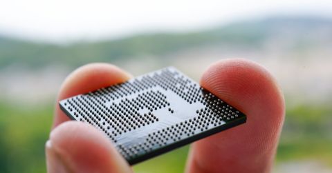
Designing a custom PCB and using a rapid prototyping service to build a functional prototype does not address the most time-consuming portion of most designs: the PCB design phase! The faster designers can iterate through prototypes, the faster the product can improve and eventually get to market.
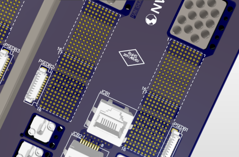
One option to build a proof of concept, intermediate prototype, or even a final product is to leverage embedded systems modules like Raspberry Pi and Arduino. There is an incredible range of modules that add complex capabilities, and the designer only needs to create a baseboard that links their modules together rather than designing everything from scratch. These modules also typically come with preconfigured drivers and sample code, which further accelerates the design process.

Custom Raspberry Pi carrier board viewed in Altium 365.
Now, instead of each PCB prototype design iteration taking months, designers can quickly adjust their designs by introducing a new module. Eventually, the embedded development and hardware converge to a final design, and the team can move on to creating a custom PCB. This can be a big cost saver, especially in hardware that leverages embedded applications.
Design tools like Upverter Modular (previously known as Geppetto) also allow designers to take off-the-shelf boards from prototype to production, even if a designer isn't well-versed in PCB layout and manufacturing. Upverter’s intuitive drag-and-drop GUI interface walks you through the process of designing a custom SBC or a carrier board that integrates all of the features your application requires.

Designing a custom PCB in Upverter Modular.
Once your design is complete in Upverter, you can download the PCB source files and complete the PCB layout on your own, or you can order directly from Upverter. You can also convert the design into Altium Designer's format as a migration, and you can complete the PCB layout on your own.
Do the Math
Having a good idea is merely the first step in a long chain of design processes. Ideas must be taken through proof of concept, optimized, and then redesigned for manufacturability. Each of these stages typically requires several evolving prototypes that implement the idea in an increasingly more efficient way.
When an iterative cycle takes months, you can only get a handful of iterations in a year. When an iterative cycle is hours or days, you can iterate effectively without limitation. For some designers, they will be able to completely implement an idea in the time it would normally take to go through a single prototype iteration. Other designers will embrace the speed of rapid prototyping to test out many different implementations and narrow in on the best product possible. With rapid prototyping, designers can bring a superior product to market faster.
We have only scratched the surface of what’s possible with Altium Designer on Altium 365. Start your free trial of Altium Designer + Altium 365 today.

关于作者
相关资源
目录
从设计到发布,全程无阻碍
- 让评审始终关联到正确的版本
- 减少交接中的混乱和返工
- 更早发现采购与发布风险
- 可独立工作,按需共享
开始使用
Thank you, you are now subscribed to updates.


 沪公网安备 31010502006411号