


What is an Engineering Bill of Materials in Agile PCB Design?

At a Glance
Why do you need an engineering bill of materials as part of your agile PCB design workflow? Here’s how you can make sense of your system with an EBOM.


If you’ve ever prepared a new device for manufacturing, then you’re probably familiar with the different types of bills of materials. Each document has its place in the design and production planning process. If you understand the role of each type of bill of materials, you can take advantage of the information it contains to improve your design process.
If you’re an agile hardware development team, then you know that your design team will need to spend time gathering and documenting functional and material requirements for your new system. An engineering bill of materials can be quickly generated with the right PCB design software and can help streamline your agile design methodology.
Key Takeaways
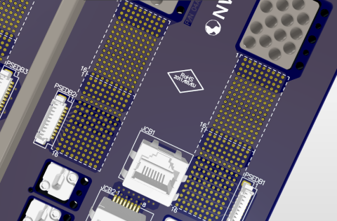
- An engineering bill of materials (EBOM) captures the original, schematic-linked definition of a PCB design, including all components, quantities, reference designators, and sourcing data.
- A well-structured EBOM supports agile hardware development by serving as the baseline for each design iteration and tracking changes as requirements evolve over the product lifecycle.
- Including suitable replacement components in the EBOM helps teams proactively manage obsolescence and supply chain risks before they impact layout or manufacturing.
- Integrating EBOM generation with a data management solution and PCB design tools enables automatic updates, early visibility into stock/obsolescence issues, and smoother communication across the design team.
- Platforms like Altium Develop combine PCB design, data management, and collaboration in one environment, making it easier to generate and maintain EBOMs as part of an agile PCB workflow.
What Is an Engineering Bill of Materials?
A bill of materials, as its name suggests, is a document that contains all part numbers, quantities, reference designators, and sourcing information for components that will appear in a new product. This document is essential for making the transition from design to manufacturing and acts as an important piece of documentation for your new product. There are many different types of bills of materials, including configurable, manufacturing, and multi-level bills of materials.
Within PCB design, an engineering bill of materials reflects the state of a system as it was originally designed. This document is just one part of a complete documentation package that should be generated as your team designs a PCB for a new electronics system. This allows a design team to view a complete list of components required to layout and manufacture a system as it was originally desired by the end customer.
As an important document in PCB design, your engineering bill of materials must link back to your original schematic. This provides a baseline design from which design teams can begin to layout a board and make modifications as needed. Your engineering bill of materials should also include lists of suitable replacement components in order to preempt obsolescence or supply chain problems that may arise later during the design process.
Device requirements typically change over a product’s lifecycle, and these changes need to be tracked during each iteration of an agile design process. Within agile PCB design, as you update your schematics and PCB layout to accommodate new or modified customer requirements, you’ll need to keep track of changes during each design sprint as part of a comprehensive quality assurance process.
Each of these components and replacements should be documented in an engineering bill of materials
An Engineering Bill of Materials in an Agile PCB Workflow
The initial state of the system can be documented as an engineering bill of materials immediately from your initial set of schematics using a schematic capture tool. This will list all the information you need to identify each component in your board, reference designators for each component, suitable replacement components, and supplier information for each component. This provides a baseline design from which to make improvements.
Once you have your initial schematic or set of hierarchical schematics, you can also start creating an initial layout for your design, assuming your schematic passes all electronic rules checks. After creating these documents and generating your engineering bill of materials, it may be a good idea to try to identify any soon-to-be obsolete or unsourceable components in the current design and substitute them with suitable replacements before you move much farther along in the design process. You can then communicate these roadblocks with your design team and explain any required design changes to the customer before you proceed further.
While this example illustrates one way to use an engineering bill of materials, it also illustrates some of the important aspects of agile methodologies. Small changes to your workflow and open communication can help you identify problems early, and help you devise quick solutions that both meet the customer’s needs and can be fully understood by your fellow designers.
If you can quickly identify any redesigns that may be required to accommodate your desired functionality, you can quickly update the product’s functional requirements and reduce the extent of redesigns. This all relies on accurate documentation and open communication with everyone involved in product development. An engineering bill of materials is just one method to provide designers with the information they need to address design changes early in the design process.
Generating an Engineering Bill of Materials With a Data Management Solution
Working with a data management solution that integrates with your PCB design software allows you to quickly identify obsolescence and supply chain problems early in the design process. This also allows you to immediately import design data updates into your engineering bill of materials, schematics, PCB layout, and other documentation. This level of data availability and the ability to quickly import data updates into your design documents helps streamline any PCB design workflow, including agile workflows.
When your data management platform is integrated alongside your standard and advanced PCB design tools, you can easily generate an engineering bill of materials and other important documentation as part of an agile PCB design process. Altium Develop integrates the powerful data management and collaboration features, providing a complete PCB design and management solution in a single platform.
Whether you need to build reliable power electronics or advanced digital systems, Altium Develop unites every discipline into one collaborative force. Free from silos. Free from limits. It’s where engineers, designers, and innovators work as one to co-create without constraints. Experience Altium Develop today!

关于作者
相关资源
目录
从设计到发布,全程无阻碍
- 让评审始终关联到正确的版本
- 减少交接中的混乱和返工
- 更早发现采购与发布风险
- 可独立工作,按需共享
开始使用
Thank you, you are now subscribed to updates.


 沪公网安备 31010502006411号