


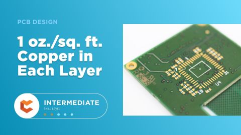


What PCB Copper Thickness Should You Use?

At a Glance
Do you know what PCB copper thickness you should use in your circuit board? Learn more about 0.5 oz/sq ft or 1.0 oz/sq ft copper thickness standards and what it means for your fabrication process in this guide.


If you’re an electronics designer or you’re just beginning your career as an engineer, the PCB stackup is probably one of the last things you’ll think about. I’ve seen professional designers jump into a new design with full force and enthusiasm, only to end up totally forgetting about some of the critical board stackup details. Simple items like PCB copper thickness and board thickness can get pushed to the back burner, but you’ll need to think about these two points for many applications as not every board will be fabricated on a standard 1.57 mm two-layer PCB.
One important point to consider in your stackup isn’t just your PCB dielectric thicknesses and the total board thickness, but also the copper thickness. The copper thickness does add to the total thickness on the outer layers alongside the solder mask, so it isn’t a trivial point to consider. So when should you opt for thicker copper than the standard value set by your fabricator? There are some situations and guidelines to consider if your design will venture outside the typical values seen in many designs.
How to Select PCB Copper Thickness
As I mentioned above, you don’t always need to specify a copper thickness other than a standard value. The typical PCB copper thickness on a copper-clad laminate will be 0.5 oz/sq ft or 1.0 oz/sq ft, although they can generally procure heavier copper as needed, or they can plate up exposed copper to a desired thickness if needed. These additional processing steps or materials will require some additional costs and time, but they are not so difficult that any PCB fabricator can’t handle such an order.
When we refer to “thickness”, we’re really talking about the weight of copper used in the board. The table below shows a helpful conversion chart between copper thickness values in mils, microns, and weight.
|
|
|
|
|
|
|
|
|
|
|
|
|
|
|
|
|
|
|
|
Although the above table only goes up to 3.0 oz/sq ft, you can go much heavier. Some fabricators offer extremely heavy copper with weights up to 20 oz/sq ft (26.8 mils or 0.34 mm PCB copper thickness).
0.5 oz/sq ft or 1.0 oz/sq ft copper thickness?
So you’re probably wondering, is the standard copper weight specified as 0.5 oz/sq ft or 1.0 oz/sq ft, or does this copper thickness difference really matter? The fact is that, for designs that would only need 0.5 oz. or 1.0 oz, the electrical distinction between the two is negligible. There is no “standard” copper thickness; some fabricators will put 1.0 oz/sq ft in their stackups, and some will put 0.5 oz/sq ft, and they may mix them on different layers. If you know who you will use to fabricate your board, take a look at their standard stackup. You can usually ask them to substitute a different thickness if you need it.
The main difference between these values (or any other copper thickness) is the DC resistance; making the copper foil thicker makes the DC resistance of your traces and planes smaller. If you need to distribute DC power across a large circuit board, then you might experience a few mV of voltage drop between your power regulator output and your load component/circuit. This becomes important again because that lost power can get dissipated as heat, and this will be one of the factors that determines temperature rise in your board. We’ll look at this more below.
Why Would You Use Heavy Copper in a PCB?
Not everyone needs heavy copper, but you may need it if you’re building high current boards, or a board that needs to operate at high temperature. To help you determine the amount of heavy copper you need, the IPC has developed some standards relating current limits, desired temperature rise, and copper thickness/width:
- Use IPC-2221 for plane thickness: There is an empirical formula published by IPC-2221 that can be used to calculate the cross-sectional area needed to determine your plane thickness. Learn more about PCB power plane thickness in this article.
- Use the IPC-2152 nomograph for traces: This table helps you calculate a required PCB trace width for a desired current, temperature rise, and copper weight, or vice versa. You can find a link to this table and an explanation in this article.
Once you’ve determined the required thickness of your copper layer, you can use the table shown above to get the required copper weight to meet your design requirements.
Specifying PCB Copper Thickness
When you’ve finished your PCB and you want to make sure your fabricator understands your design data, including copper weight, make sure you specify this data to your manufacturer. There’s an important point to note here: your Gerber files will not specify your copper thickness. Gerber files are only in 2D, not in 3D. Instead, you should put this information into a stackup table in fabrication drawings, or you should at least generate a board layer stackup report you can send to your fabricator:
- Export a DXF file for your drawings: If you have a program like AutoCAD or another drawing program, you can import a DXF file into a template and generate a drawing file. You can then export this to a PDF and send it off to your fabricator.
- Create a Board Stack Report: Not all ECAD software will automate creation of this drawing. Professional design tools can quickly generate it as a PDF or Excel file, and you can send this to your fabricator while you’re planning your board, or before you submit your design for quote.

The Board Stack Report shown above is the same type of drawing your fabricator will send you if you request a review of your design early. It may include some additional details on certain layers, such as the width required for a specific impedance target. If you need to use heavy copper, make sure you communicate this to your fabricator early so they can help ensure you follow the required design rules.
When you need to access an easy-to-use PCB layout tool that includes everything needed to build high-quality manufacturable circuit boards, look no further than CircuitMaker. After you’ve determined your required PCB copper thickness and you’re planning for manufacturing, you can instantly generate the output files needed by PCB fabricators. All CircuitMaker users also have access to a personal workspace on the Altium 365 platform. You can upload and store your design data in the cloud, and you can easily view your projects via your web browser in a secure platform.
Start using CircuitMaker today and stay tuned for the new CircuitMaker Pro from Altium.

关于作者
Related Technical Documentation
相关资源
目录
从设计到发布,全程无阻碍
- 让评审始终关联到正确的版本
- 减少交接中的混乱和返工
- 更早发现采购与发布风险
- 可独立工作,按需共享
开始使用
Thank you, you are now subscribed to updates.


 沪公网安备 31010502006411号