Skip to main content
Mobile menu
Altium Develop
资源 & 支持中心
Altium 365 免费工具
Gerber Compare
在线 PCB 查看器
了解产品
下载
联系我们
关注微信
扫描二维码
关注Altium微信平台
资源 & 支持中心
所有资源
支持中心
文档
官方直播
Altium 社群
社群
Bug提交
创意
教育
学生实验室
教育者中心
Altium 教育课程
Search Open
Search
Search Close
登录
Home
Main menu
首页
PCB设计
团队协作
元器件创建
PCB数据管理
PCB设计输出和文档
ECAD/MCAD
HDI设计
高速设计
多板设计
PCB布局
PCB布线
PCB供应链
电源完整性
RF设计
刚柔结合板PCB设计
原理图输入
信号完整性
PCB设计仿真/分析
软件
Develop
Discover
Agile
Altium的365
Altium Designer的
资源中心
项目
Altium Academy
工程新闻
指南书
新闻通讯
播客
项目
培训课程
网络研讨会
白皮书
Overview
All Content
CoDesign and CoEngineering (ECAD/MCAD Collaboration)
Component Management and Libraries
Data Management and Version Control
Manufacturing Outputs and Compliance
PCB Design and Layout
Supply Chain and Component Sourcing
Systems and Product Design
Filter
清除
Role
全部
ECAD 库管理员
电气工程师
工程经理
IT 经理
机械设计工程师
PCB 设计工程师
采购经理
软件工程师
Software
全部
开发
敏捷
Altium Designer
Altium 365
Assembly Assistant
BOM Portal
PLM集成
GovCloud
Jira Integration
Octopart
Requirements Portal
Content Type
全部
指南
网络研讨会
视频
播客
白皮书
Region
全部
7 Common Misconceptions about PCB Design
5 min
Thought Leadership
After years of PCB assembly, you probably know about a decoupling capacitor, a solder mask, and schematic symbols like the
阅读文章
How to Easily Import Your Designs to Your Favorite Design Tools
3 min
Thought Leadership
One task that has always proven difficult is moving electronic product designs from one printed board design software environment to
阅读文章
How to Automate Your Design Review Workflow and Process
2 min
Blog
Your typical design review workflow can be filled with endless hurdles, errors, and time-consuming processes without the right tools, but
阅读文章
Personalizing Your Altium Designer Experience
3 min
Thought Leadership
The “one-stop-shop” approach to electronics design provides engineers with all the PCB software they need, all at their fingertips. However
阅读文章
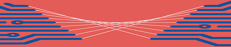
How to Simplify Your Routing with Pin Swapping
3 min
Thought Leadership
Optimal component placement goes a long way towards minimizing crossover connection lines. However, crossovers can never be completely avoided. Learn
阅读文章
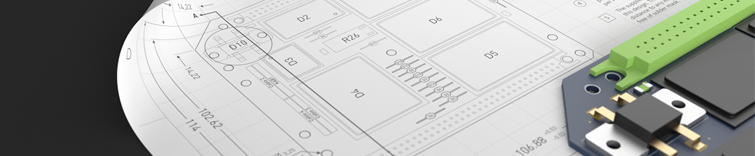
Draftsman: Make the Software Do the Documentation
6 min
Blog
You’ve routed your last route. Stitched your last via. Poured your last pour. You’re finally done with that board —
阅读文章
Bugging Out - How to Minimize Your Embedded Design Debug Phase
6 min
Thought Leadership
Even if not all engineers will admit it, debugging an embedded system prototype is a lot of fun, so long
阅读文章
Pagination
First page
« First
Previous page
‹‹
页面
1154
当前页面
1155
页面
1156
页面
1157
页面
1158
页面
1159
Next page
››
Last page
Last »


 沪公网安备 31010502006411号