Skip to main content
Mobile menu
Altium Develop
资源 & 支持中心
Altium 365 免费工具
Gerber Compare
在线 PCB 查看器
了解产品
下载
联系我们
关注微信
扫描二维码
关注Altium微信平台
资源 & 支持中心
所有资源
支持中心
文档
官方直播
Altium 社群
社群
Bug提交
创意
教育
学生实验室
教育者中心
Altium 教育课程
Search Open
Search
Search Close
登录
Home
Main menu
首页
PCB设计
团队协作
元器件创建
PCB数据管理
PCB设计输出和文档
ECAD/MCAD
HDI设计
高速设计
多板设计
PCB布局
PCB布线
PCB供应链
电源完整性
RF设计
刚柔结合板PCB设计
原理图输入
信号完整性
PCB设计仿真/分析
软件
Develop
Discover
Agile
Altium的365
Altium Designer的
资源中心
项目
Altium Academy
工程新闻
指南书
新闻通讯
播客
项目
培训课程
网络研讨会
白皮书
Overview
All Content
CoDesign and CoEngineering (ECAD/MCAD Collaboration)
Component Management and Libraries
Data Management and Version Control
Manufacturing Outputs and Compliance
PCB Design and Layout
Supply Chain and Component Sourcing
Systems and Product Design
Filter
清除
Role
全部
ECAD 库管理员
电气工程师
工程经理
IT 经理
机械设计工程师
PCB 设计工程师
采购经理
软件工程师
Software
全部
开发
敏捷
Altium Designer
Altium 365
Assembly Assistant
BOM Portal
Cloud PLM Connector
PLM集成
GovCloud
Jira Integration
Octopart
Requirements Portal
Content Type
全部
指南
网络研讨会
视频
播客
白皮书
Region
全部
Create and Simulate in a Unified Design Environment
2 min
Webinars
Leveraging circuit simulation in the schematic capture environment is a powerful tool that enables projects to be completed sooner and
阅读文章
Create and Simulate in a Unified Design Environment
2 min
Webinars
Leveraging circuit simulation in the schematic capture environment is a powerful tool that enables projects to be completed sooner and
阅读文章
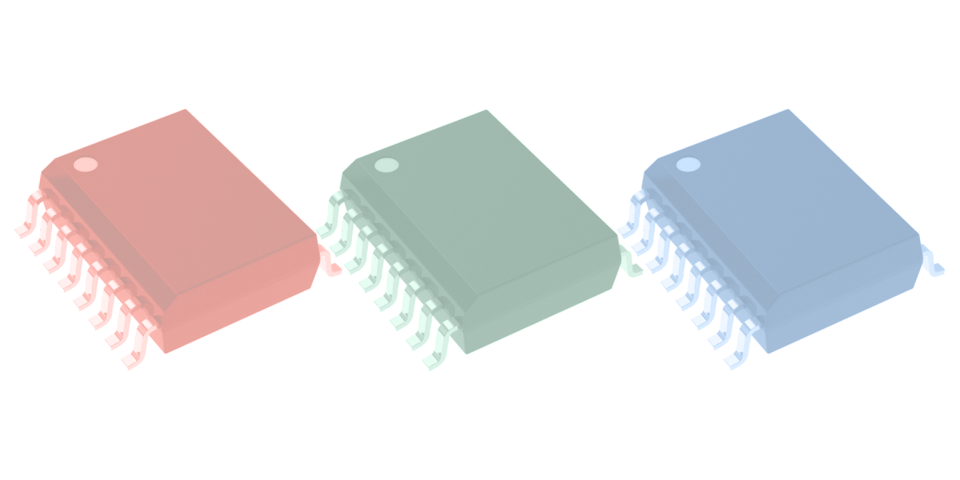
隔离式CAN收发器IC用于高速数字通信
1 min
Guide Books
想象一下,如果你的汽车中的电子设备需要一对线缆来相互连接。汽车中的电缆组装已经相当庞大,但CAN总线是帮助减少总线宽度和线缆数量的协议之一。尽管最初是由大型制造商而不是汽车工业采用的,CAN总线仍然是汽车领域的重要部分,并在建筑自动化等领域找到了用途。 本质上,任何需要在单个串行总线上连接多个设备并且可以延伸很长距离的系统都可以使用CAN总线。使其成为可能的是一种特殊的收发器,它为总线的其余部分提供逻辑信号。工业、汽车、机器人等应用可能需要隔离的CAN收发器,这取决于最终子系统的位置。以下是您需要使用隔离CAN收发器的情况以及您在市场上可以找到的示例组件。 理解CAN总线 控制器局域网络(CAN)总线最初由博世(Bosch)开发,并最终在ISO 11898标准中得到规范。这种架构非常简单,尽管对于初学者来说,数据帧的构建可能会有些困难。总线上的每个设备都使用一个收发器,然后向总线上每个其他设备的收发器传输和接收消息。一个基本的识别功能确保网络上只有期望的节点实际处理接收到的数据。下面展示了典型的CAN总线结构。 每个节点上都有收发器的CAN总线架构。 CAN总线协议中使用的标准功能包括一系列数据速率、错误处理、冲突检测和容错能力。在这个总线中,我们有一个可以跨越长距离的双线系统,具体取决于数据速率。CAN标准定义的数据速率和最大距离如下所示。请注意,最后一项是在CAN FD规范(ISO 11898-2)中定义的;这个标准允许将更多数据打包进单个帧中(64字节对比经典CAN的8字节)。 一些最初在工业控制和通信中的应用可能涉及在高电压源附近工作,因此需要隔离来保护系统组件。您可以使用CAN收发器IC,而不是使用外部变压器来取消共模瞬态。 为什么使用隔离的CAN收发器? 隔离的CAN收发器IC集成了与CAN总线接口所需的标准功能,同时确保高电隔离。由于汽车、航空航天和一系列工业应用需要在高电压源附近或可能的电源浪涌附近工作,隔离的CAN收发器是确保可靠性的理想选择。 因为您需要在隔离与数据速率及其他集成特性之间取得平衡,所以请注意这些重要规格: 隔离等级。隔离是使用这类收发器的主要原因,它们的 ESD等级对于确保安全性和与其他产品及特定应用的兼容性非常重要。这通常以kV范围的RMS值表示。 故障电压。电气故障可能发生在总线上,而不是由外部电源引起的。对于高质量组件,故障电压通常为几十伏。 温度等级。由于CAN总线通常部署在较为恶劣的环境中,它们可能需要较高的温度要求。请务必在您的组件数据表中检查此项。 标准合规性。像许多电源管理组件一样,隔离CAN收发器的数据表可能包含合规性声明。UL 1577是一个常见标准,但如果收发器针对特定应用,也可能列出IEC标准或ISO标准。 以下是您会从组件制造商和分销商那里找到的一些常见CAN收发器IC。
阅读文章
用于硬件开发的 Jira:工具与流程
1 min
Blog
PCB 设计工程师
Engineering Teams
使用 Jira 开展硬件开发,实现更清晰的工作流程、评审和可追溯性。了解 Jira 与 GitHub 的对比,以及如何填补 PCB 数据缺口。
阅读文章
Common Printed Circuit Board Defects You Can Fix in the Cloud
7 min
Thought Leadership
Solve these printed circuit board defects you can fix with the cloud collaboration tools in Altium Designer.
阅读文章
Create and Simulate in a Unified Design Environment
1 min
Webinars
Leveraging circuit simulation in the schematic capture environment is a powerful tool that enables projects to be completed sooner and
阅读文章
Rochester Electronics 关于2021年半导体市场动态
1 min
Blog
编者按:以下内容由 Rochester Electronics 与Octopart合作撰写。 高管对长交货期的看法 半导体市场正从过度库存期转向延长的交货期、短缺和可能的分配问题 - 这对您意味着什么? 半导体行业以其周期性而闻名。自1981年Rochester Electronics成立以来,我们大约经历了19个不同程度的行业周期。 每个周期的原因可能不同。它们都倾向于突然开始并突然结束,确实可能会给人这种感觉。 我们行业中越来越多的声音表明,我们即将进入一个供应紧张的市场。越来越多关于这个话题的文章浮出水面,直接描述了影响汽车制造商的问题,例如。因此,我们可能开始看到更广泛的下游效应,因为相同的组件往往有许多用途。 这种潜在转变的一个关键区别是,它并非发生在全球经济繁荣的背景下。事实上,恰恰相反。在我们当前前所未有的环境中,预测结果更加具有挑战性。它会是短期的,迅速被(经常看到的)过度库存所取代,对应着经济需求的疲软,导致市场下滑吗?或者它会因基于全球经济复苏的强劲需求而被延长和加剧,作为克服COVID的结果? 实际上,许多事情我们无法控制。然而,我相信我们都希望COVID能够迅速结束,包括经济增长和就业创造在内的正常状态能够恢复。 让我们谈谈我们能控制的事情。 在这样的时期,“坏分子”会出现在市场上,利用那些感觉无处可去的买家。次标和假冒产品开始出现,使不知情的买家处于潜在的高风险情况。通过仅从完全授权的来源购买 活跃和/或生命周期末期的组件,如Rochester Electronics,避免这种风险。 完全 授权的分销商符合SAE航空航天标准AS6496。简单来说,他们被原始组件制造商(OCM)授权提供可追溯和保证的产品,
阅读文章
Pagination
First page
« First
Previous page
‹‹
页面
305
当前页面
306
页面
307
页面
308
页面
309
页面
310
Next page
››
Last page
Last »


 沪公网安备 31010502006411号