Skip to main content
Mobile menu
Altium Develop
资源 & 支持中心
Altium 365 免费工具
Gerber Compare
在线 PCB 查看器
了解产品
下载
联系我们
关注微信
扫描二维码
关注Altium微信平台
资源 & 支持中心
所有资源
支持中心
文档
官方直播
Altium 社群
社群
Bug提交
创意
教育
学生实验室
教育者中心
Altium 教育课程
Search Open
Search
Search Close
登录
Home
Main menu
首页
PCB设计
团队协作
元器件创建
PCB数据管理
PCB设计输出和文档
ECAD/MCAD
HDI设计
高速设计
多板设计
PCB布局
PCB布线
PCB供应链
电源完整性
RF设计
刚柔结合板PCB设计
原理图输入
信号完整性
PCB设计仿真/分析
软件
Develop
Discover
Agile
Altium的365
Altium Designer的
资源中心
项目
Altium Academy
工程新闻
指南书
新闻通讯
播客
项目
培训课程
网络研讨会
白皮书
Overview
All Content
CoDesign and CoEngineering (ECAD/MCAD Collaboration)
Component Management and Libraries
Data Management and Version Control
Manufacturing Outputs and Compliance
PCB Design and Layout
Supply Chain and Component Sourcing
Systems and Product Design
Filter
清除
Role
全部
ECAD 库管理员
电气工程师
工程经理
IT 经理
机械设计工程师
PCB 设计工程师
采购经理
软件工程师
Software
全部
开发
敏捷
Altium Designer
Altium 365
Assembly Assistant
BOM Portal
Cloud PLM Connector
PLM集成
GovCloud
Jira Integration
Octopart
Requirements Portal
Content Type
全部
指南
网络研讨会
视频
播客
白皮书
Region
全部
What is Transfer Impedance in a PDN?
10 min
Blog
We talk about signal integrity and power integrity a lot on this blog. Both are important concepts and are related
阅读文章
Best Practices: Efficient Use of Snapping in Altium Designer
23 min
Webinars
Getting your PCB layout design done takes patience and precision. Complex footprint geometries, board shape, and dense component placement require
阅读文章
Coming Soon: Altium CircuitMaker Pro®
2 min
Engineering News
In 2015, Altium released Altium CircuitStudio® to best meet the needs of casual users, hobbyists, students, and PCB design aficionados on a budget. Learn about the new version coming to the public!
阅读文章
How the Open Source Ventilator Project Went from Design to Build in Record Time
2 min
Podcasts
Dugan Karnazes (Velocity Research), Rob Cooke (Calumet Electronics), and Chris Denney (Worthington Assembly) join the OnTrack podcast to relay their experiences while working on the OSV (Open Source Ventilator) project.
阅读文章
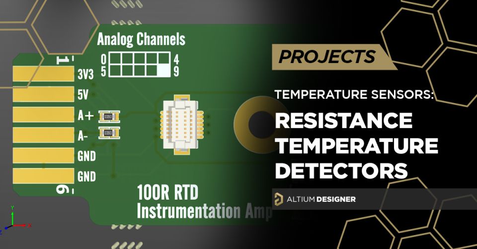
Temperature Sensor Project: Resistance Temperature Detectors (RTD)
20 min
Altium Designer Projects
In this part of the series, we’re looking at Resistance Temperature Detectors (RTD), which are among the most accurate temperature measuring elements we have easy access to.
阅读文章
Announcing the Official Altium Brand Store
1 min
Newsletters
We've been asked by everyone from customers to AltiumLive attendees to employees for real, branded Altium merchandise for years. We’ve
阅读文章
Spotting DDR4 Impedance Violations in High Speed PCB Design
8 min
Blog
DDR4 is one of many high speed interfaces that requires impedance control during routing. If you can spot impedance discontinuities, you can prevent excess insertion/return losses in leading to your DDR4 memory modules.
阅读文章
Pagination
First page
« First
Previous page
‹‹
页面
349
当前页面
350
页面
351
页面
352
页面
353
页面
354
Next page
››
Last page
Last »


 沪公网安备 31010502006411号