Skip to main content
Mobile menu
Altium Develop
资源 & 支持中心
Altium 365 免费工具
Gerber Compare
在线 PCB 查看器
了解产品
下载
联系我们
关注微信
扫描二维码
关注Altium微信平台
资源 & 支持中心
所有资源
支持中心
文档
官方直播
Altium 社群
社群
Bug提交
创意
教育
学生实验室
教育者中心
Altium 教育课程
Search Open
Search
Search Close
登录
Home
Main Chinese menu
首页
PCB设计
团队协作
元器件创建
PCB数据管理
PCB设计输出和文档
ECAD/MCAD
HDI设计
高速设计
多板设计
PCB布局
PCB布线
PCB供应链
电源完整性
RF设计
刚柔结合板PCB设计
原理图输入
信号完整性
PCB设计仿真/分析
软件
Altium Designer的
资源中心
工程新闻
指南书
网络研讨会
Overview
All Content
CoDesign and CoEngineering (ECAD/MCAD Collaboration)
Component Management and Libraries
Data Management and Version Control
Manufacturing Outputs and Compliance
PCB Design and Layout
Supply Chain and Component Sourcing
Systems and Product Design
Filter
清除
Role
全部
ECAD 库管理员
电气工程师
工程经理
IT 经理
机械设计工程师
PCB 设计工程师
采购经理
软件工程师
Software
全部
Develop
Agile
Altium Designer
Altium 365
Assembly Assistant
BOM Portal
PLM集成
GovCloud
Jira Integration
Octopart
Requirements Portal
Content Type
全部
指南
网络研讨会
视频
播客
白皮书
Region
全部
蓝牙5微控制器选择指南
1 min
Guide Books
小型蓝牙5微控制器模块 蓝牙5自2016年以来一直伴随着我们,而5.1版本仅在一年前发布。相比于前代,升级后的协议提供了许多改进。与此同时,我们见证了不同组件在系统级芯片(SoCs)中的更大整合,而蓝牙5/5.1也不例外。如果你正在开发一个轻量级产品,对计算要求不高且需要长期运行,那么蓝牙5微控制器是运行你的新产品的绝佳组件。 蓝牙5特性 蓝牙5规范及新一代蓝牙5.1提供了更长的范围、更高的数据速率和比以往代更低的功耗。蓝牙的一个主要卖点是其用于在短距离内配对多个设备,但是一级蓝牙5设备配备独立电源,在工业用途中的评级可达330英尺。蓝牙5还引入了一个可选的无线电PHY,称为‘LE Coded’,在1 Mbps下最大TX功率可达+20dBm。这相当于潜在的4倍范围增加。 对于工业空间之外的典型物联网设备,如可穿戴设备和智能家居产品,你所需的大部分或全部功能很可能直接集成在蓝牙5微控制器中。这些组件因为它们所提供的集成而变得越来越受欢迎,用于轻量级和 工业应用。 选择蓝牙5微控制器 蓝牙5微控制器是高度集成的产品,将包括大量的GPIO连接,以及许多其他集成的外设。示例包括集成的音频编解码器、PWM输出、高精度ADC和可配置接口。射频前端也集成在这些组件中,一些设备将包括集成的天线。以下是选择蓝牙5微控制器时需要考虑的一些重要点: 数据流速率:数据速率可达2 Mbps,尽管一些定制的SoC可能会超过这个速度。 供电电压范围:如果您正在处理移动设备,它将使用电池供电,电池电压会随着时间逐渐下降。当电压过低时,设备将关闭,任何未保存的数据将丢失。 板载内存:这包括板载Flash内存和板载RAM。较重的计算工作负载将需要更大的板载RAM。蓝牙5微控制器倾向于拥有1 MB或更少的板载Flash内存,因此这些产品的代码需要进行大量优化。microSD卡是扩展产品内存的好选择。 全功率发送时的电流:如果您的产品将数据流式传输到另一设备,全功率发送时的电流将决定您的电池续航时间。这为操作期间的电池寿命设定了一个下限。典型值为5-10 mA。 睡眠模式下的电流:当设备不在积极处理数据或接收输入时,可以进入睡眠模式。这个值的范围从约1 μA到约100 nA,用于保持RAM中的数据。
阅读文章
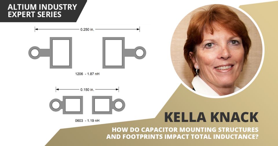
How Do Pads and Vias Impact Total Capacitor Parasitic Inductance?
9 min
Blog
In this blog article we discuss how the footprint and mounting style affect capacitor parasitic inductance. The pads and vias back to the PCB power planes increase the total series inductance of the capacitor.
阅读文章
Draftsman and FAB/Assembly File Generation | Altium Academy Live
1 min
Webinars
In this session, we will cover Draftsman for design documentation, FAB/Assembly house file generation and automating their creation using Outjobs.
阅读文章
2:26:15
Altium Academy Virtual Sessions: Tech Track - DDR and BGA Routing and Fanout Webinar
1 min
Webinars
This tech track will discuss DDR and BGA Routing Best Practices and addresses the challenges to the designer and illustrates
阅读文章
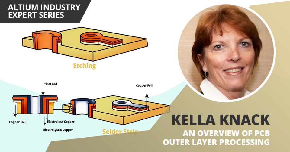
An Overview Of PCB Outer Layer Processing
5 min
Thought Leadership
Expert Kella Knack describes in detail the fabrication of the PCB outer layer. Read and learn about how different vias are formed and the steps involved in the multilayer build-up process.
阅读文章
The PCB Fabrication Process—What Every Design Engineer Needs To Know, Part 2
15 min
Blog
In Part 1 of this article, I described the first steps that occur during the PCB fabrication process. They detailed
阅读文章
The PCB Fabrication Process—What Every Design Engineer Needs To Know, Part 1
11 min
Blog
In the olden and not-so-olden days of PCB development, the process of moving a board from design to manufacturing was
阅读文章
Pagination
First page
« First
Previous page
‹‹
页面
384
当前页面
385
页面
386
页面
387
页面
388
页面
389
Next page
››
Last page
Last »


 沪公网安备 31010502006411号