Skip to main content
Mobile menu
Altium Develop
资源 & 支持中心
Altium 365 免费工具
Gerber Compare
在线 PCB 查看器
了解产品
下载
联系我们
关注微信
扫描二维码
关注Altium微信平台
资源 & 支持中心
所有资源
支持中心
文档
官方直播
Altium 社群
社群
Bug提交
创意
教育
学生实验室
教育者中心
Altium 教育课程
Search Open
Search
Search Close
登录
Home
Main menu
首页
PCB设计
团队协作
元器件创建
PCB数据管理
PCB设计输出和文档
ECAD/MCAD
HDI设计
高速设计
多板设计
PCB布局
PCB布线
PCB供应链
电源完整性
RF设计
刚柔结合板PCB设计
原理图输入
信号完整性
PCB设计仿真/分析
软件
Develop
Discover
Agile
Altium的365
Altium Designer的
资源中心
项目
Altium Academy
工程新闻
指南书
新闻通讯
播客
项目
培训课程
网络研讨会
白皮书
Overview
All Content
CoDesign and CoEngineering (ECAD/MCAD Collaboration)
Component Management and Libraries
Data Management and Version Control
Manufacturing Outputs and Compliance
PCB Design and Layout
Supply Chain and Component Sourcing
Systems and Product Design
Filter
清除
Role
全部
ECAD 库管理员
电气工程师
工程经理
IT 经理
机械设计工程师
PCB 设计工程师
采购经理
软件工程师
Software
全部
开发
敏捷
Altium Designer
Altium 365
Assembly Assistant
BOM Portal
Cloud PLM Connector
PLM集成
GovCloud
Jira Integration
Octopart
Requirements Portal
Content Type
全部
指南
网络研讨会
视频
播客
白皮书
Region
全部
1:11:50
GMT20190815-170031_Altium-Con_3840x2160
1 min
Webinars
阅读文章
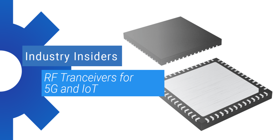
无线连接中的RF收发器用于5G和物联网设备
1 min
Guide Books
物联网(IoT)的实现仅通过使用无线通信技术作为介质连接人、物、地点乃至动物到互联网之间的互联互通而成为可能。使用IoT设备的一个主要优势是直接传输和持续共享数字数据。同样,它对不同领域如交通、健康、天气和环境监测产生了重大影响。 当谈到互联网连接时,有一些设备会立即浮现在我们的脑海中;我们的智能手机、个人电脑、平板电脑、台式机等。它们已经被构建具有连接到互联网的能力,并通过这样做,交换数据和信息。但还有其他一些智能设备原本并不打算具有互联互通性。RF组件为这些设备提供无线连接,使它们能够像计算机和智能手机一样远程通信和工作。 频率和协议 频率和无线通信协议将决定任何IoT设备所需的相关组件。这两个因素共同提供在特定频段内的无线通信。任何无线设备都需要一个无线收发器芯片才能操作并按预期功能。许多IoT设备通过Wifi、 ZigBee、蓝牙或其他协议在GHz频率范围内通信。 一些收发器可以根据需要在单个设备内数字重新配置以支持不同的协议。随着即将到来的5G支持设备,收发器必须配备天线调谐开关,以提供定向传输的波束成形。放大器和滤波器是包括IoT设备在内的多种设备中至关重要的RF组件。功率放大器和微弱信号放大器主要用于IoT设备。微弱信号放大器用于无线收发器的接收端,而功率放大器则用于收发器的发送端。 从您的收发器开始 您的收发器将构成您的 IoT设备无线通信能力的基石。过去需要分开的发射器、接收器和其他支持组件,一个集成的收发器IC在单一封装中提供信号调理、调制和发送/接收功能。以下是一些在各种频段操作的优秀无线收发器选项: Semtech, SX1211I084TRT 这款来自Semtech的 SX1211I084TRT收发器是一款低频收发器,工作频段为863-870、902-928或950-960 MHz,采用FSK或OOK调制。这款收发器的数据传输速率仅为FSK模式下的25 kbps或OOK模式下的2 Kbps,因此它的使用被限制在涉及较低吞吐量的应用中。一个很好的例子是来自小型无线传感器阵列的周期性数据传输。然而,这款封装的高度集成性有助于减少总体部件数量,使其非常适合用于在较低RF频率下通信的可穿戴设备: SX1211...高度集成的架构允许在保持设计灵活性的同时最小化外部部件数量。所有主要的RF通信参数都是可编程的,而且它们中的大多数可以动态设置。它符合欧洲(ETSI EN 300-220 V2.1.1)和北美(FCC
阅读文章
23
TradeInTradeUp_Q1Promo_DE
1 min
Videos
阅读文章
2019/06/22 - 2层简易四轴飞行器之PCB设计拼版及生产资料整理
1 min
Webinars
对于一个PCB设计,布局布线完成之后,整个项目基本上就算完成90%了。那么剩下的10%是什么呢?我们一般设计完成是需要发出给板厂生产的。一个好的设计是否考虑了生产制造环节的成本,是否考虑了设计的可制造性呢?这些又是从哪些方面去考虑呢?我们一起来做一个规范的工程师吧!
阅读文章
读取小信号电压
1 min
Guide Books
如果您使用过输出电压非常低的传感器,例如负载电池或其他惠斯通桥或电流变压器,您就会知道需要一个非常精确的放大器和一个高位数的模拟数字转换器(ADC)来利用它们的测量结果。我的大多数电路板都有非常严格的尺寸限制,因此集成更多组件并不总是理想的解决方案。然而,通过使用具有可编程增益放大器(PGA)的高位数ADC,您可以节省显著的板空间,并且还可以提高一批板之间读数的一致性。 负载电池中的应变计可能具有每伏特仅1mV的满量程输出,如果以5伏特运行,将为满传感器范围提供0-5mV的信号。这使得100kg的负载电池每千克提供50μV的信号,没有显著的放大就无法提供可用数据。即使有128倍的放大,满载时的信号也仅为0.64伏特,这将使您使用3.3伏特8位ADC的分辨率远非理想,大约为2kg。然而,大多数现代ARM控制器都有一个10位或12位的ADC,这将使您在负载电池上的分辨率约为125克。这仍然相当差,因此我们可以考虑使用提供更高位数的外部ADC,以获得满意的分辨率。利用24位ADC和128 V/V放大器,我们的100kg负载电池现在可以读取毫克。这种高分辨率允许进行精确测量,并且对于可能使用满量程范围为多吨的负载电池(例如:起重机,称重桥)或必须处理潜在数千安培的电流传感器(例如:办公楼,工厂)的精密工业应用至关重要。额外的分辨率还允许过滤信号以确保稳定的读数和对读数的高度信心。 可编程增益放大器 具有可编程增益放大器的ADC比同等分辨率的常规ADC稍贵,但在我的项目中证明了额外的费用是非常值得的。更不用说,使用具有精密运算放大器和精密电容器及电阻的ADC的解决方案往往与集成单元的成本相当,因此并没有真正的优势。集成的PGA解决方案还提供了显著减少的板空间,以及从板到板之间更加一致的信号放大。由于增益很容易编程,它还使得切换到不同的传感器选项非常容易,为一系列传感器提供全分辨率支持。 如果您使用的是微控制器的ADC或缺乏集成可编程增益放大器的其他外部ADC,市场上也有独立的PGA可供选择。德州仪器的 PGA281 是一个非常受欢迎的选择,可提供高达128 V/V的差分或单端信号放大。 模拟数字转换器 从上面的例子中,你可以看到,一个好的微控制器中的12位ADC对于小信号电压来说并不够用。如果你使用的是像Arduino中流行的ATmega,你只有一个8位的ADC,这限制更大。因此,需要外部ADC才能以足够的精度读取这样的小电压,以提供可用的数据。 虽然高位数很重要,但它不是唯一重要的因素。处理小电压时,你的ADC需要低漂移,有非常稳定的参考电压,并且有足够的带宽来捕获你的信号。一个不稳定或漂移的ADC即使位数很高也会给你不准确的读数。 我倾向于使用德州仪器的 ADS1220来读取电流变压器或应变计,因为它非常稳定且精度极高。它是一个24位的ADC,但是有了内部滤波器,它给你有效的20位可用分辨率。话虽如此,这就是我在我的一个项目中如何连接我的ADS1220的: 电路的实现相当关键。我有一个π滤波器,它在输入端使用了一个铁氧体珠而不是电感,如此处所示,负载细胞的输入端也有一些非常基本的滤波: 这个电路用于测量加拿大奥林匹克队使用的Omega LCM302 2000牛顿负载细胞的数据。当将记录的数据与在顶级田径力量板上记录的相同冲击波进行比较时,ADS1220的数据能够以每秒960个样本的速度更精确地读取短时冲击波,且随着温度变化,结果的信号抖动和漂移更小。 可编程增益放大器和直接从ADC供电的负载细胞使得通过配置更改放大倍数或在检测到过载时轻松切换到满量程更小的负载细胞变得简单。这使得4输入的ADS1220对我的应用来说比它稍微便宜一些的单通道兄弟ADS1246更有吸引力。 市场上还有很多其他选项,其中一些可能更适合你的特定应用,所以为什么不通过浏览ADC类别并在Octopart上搜索
阅读文章
High Density Interconnects - A Design and Manufacturing Guidebook
58 min
Guide Books
A compilation of Happy Holden's expert advice on high density interconnect design, routing, layout, and manufacturing for HDI PCBs.
阅读文章
47:30
Copy of Concord Pro- Library Management
1 min
Webinars
阅读文章
Pagination
First page
« First
Previous page
‹‹
Page
531
当前页面
532
Page
533
Page
534
Page
535
Page
536
Next page
››
Last page
Last »


 沪公网安备 31010502006411号