Bring all electronic design data together in one secure workspace.
设计过程中会产生大量的具有到期日期远远超出了设计阶段结束的数据。 Altium的探索长期和设计数据的短期安全存储,以及如何确保这个设计数据可以在未来更有效的设计做出贡献。浏览我们的资源库在PCB设计数据管理。
Watch this webinar to discover how to create different aspects of a component, including symbols, footprints and 3D model parametric data.
We are pleased to host a thought-provoking conversation between Tech Consultant Zach Peterson and Dr. Philip Voglewede. They have a very intriguing conversation about the role of automation in the current and future industrial landscape.
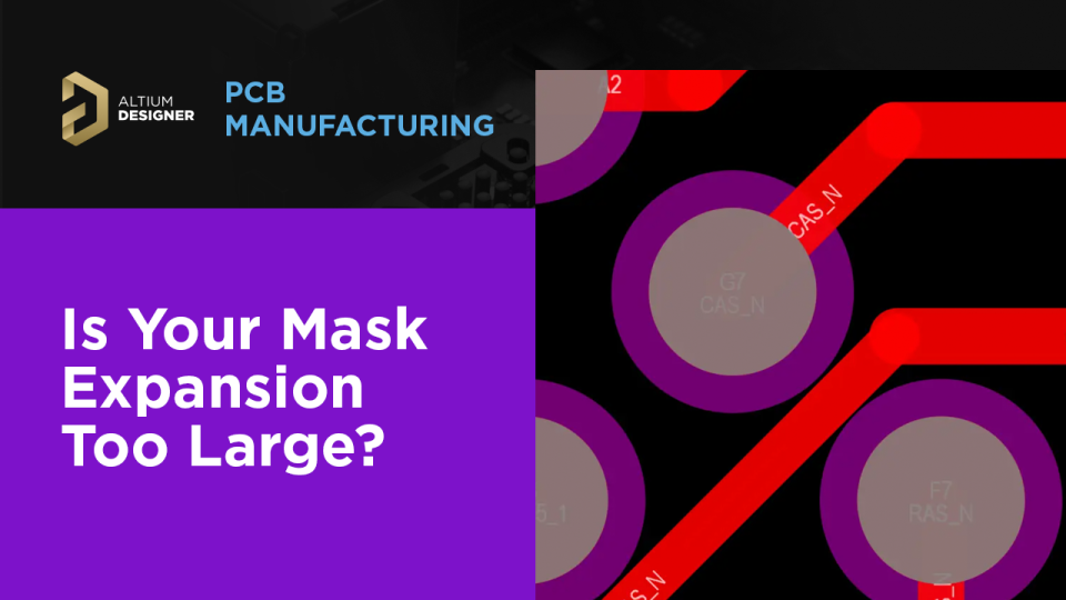
Solder mask expansion on a PCB can be set in your design rules to ensure sufficient copper is visible for soldering.
This is a very exciting conversation. We will talk with Dr. Eyal Weiss about better, practical applications of AI in the electronics industry, outside of design.
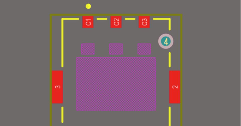
Your PCB footprints contain many layers. Which of these layers are most important and what should they contain? We’ll explore in this article.
DIP components are less-often used in professional PCB design projects for new products, but legacy products may still need these parts.