Skip to main content
Mobile menu
解决方案
Altium Develop
在 Altium Designer 中设计先进 PCB,可独立设计,也可在需要时连接评审、数据来源和发布协同。
Altium Agile Teams
在多学科电子开发与协作中引入结构化流程,确保效率与速度不受影响。
资源 & 支持中心
Altium 365 免费工具
Gerber Compare
在线 PCB 查看器
了解产品
下载
联系我们
关注微信
扫描二维码
关注Altium微信平台
资源 & 支持中心
用户指南
实战讲堂
学习中心
技术文档
支持中心
常见问题
Altium 社群
社群
Bug提交
创意
教育
学生实验室
Free access to professional PCB design software, training, and learning resources for students
教育者中心
A comprehensive education platform providing curriculum, software, training, and classroom resources for educators
Altium 教育课程
Free college- and university-level PCB design curriculum designed to prepare students for real-world engineering careers
Search Open
Search
Search Close
登录
指南
Main menu
首页
PCB设计
团队协作
元器件创建
PCB数据管理
PCB设计输出和文档
ECAD/MCAD
HDI设计
高速设计
多板设计
PCB布局
PCB布线
PCB供应链
电源完整性
RF设计
刚柔结合板PCB设计
原理图输入
信号完整性
PCB设计仿真/分析
软件
Discover
Develop
敏捷团队
敏捷企业
Altium 365
Altium Designer
资源中心
项目
Altium Academy
工程新闻
指南书
新闻通讯
播客
项目
培训课程
网络研讨会
白皮书
首页
指南
指南
Altium的指南书籍为PCB设计提供了深入的见解和教育。
Explore Altium Develop
Explore Altium Agile
Ask an Expert
Overview
Altium Develop
Agile
Altium Designer
Altium 365
Octopart
All Content
Filter
found
Sort by
Most Recent
Most Popular
Title (A-Z)
Title (Z-A)
Role
ECAD 库管理员
电气工程师
工程经理
IT 经理
机械设计工程师
PCB 设计工程师
采购经理
软件工程师
Software
Altium Develop
Altium Agile 团队
Altium Designer
Altium 365
Assembly Assistant
BOM Portal
Cloud PLM Connector
PLM集成
Configurable Workflows
Jira Integration
MCAD CoDesigner
Octopart
Requirements Portal
Content Type
指南
视频
白皮书
Altium Vault Evaluation Guide
1 min
Guide Books
To learn more about this topic please see the full solution - Evaluating Altium Vault - at Altium.com.
阅读文章
如何把PCB项目从PADS开发平台转换到Altium Designer开发平台
1 min
Guide Books
Users of Competitor Tools
本篇文章主要介绍了PCB项目在不同开发平台之间进行转换的相关信息。Altium Designer 对基于不同开发平台开发的PCB项目都可以进行无缝转换,整个转换的过程操作简单,各种平台的支持范围广泛。Altium Designer 为开发人员可以利用对不同平台的PCB项目进行二次编辑提供了极大的便利。本篇文章内容包括作为PCB设计人员在设计过程中对于开发平台本身应当关注的问题有哪些。Altium Designer 对比PADS开发平台优势在哪里,将PCB项目从PADS平台转换到Altium Designer平台主要步骤有哪些。 从PADS到Altium Designer的转换 今天的电子工程师在产品的设计中面临越来越多的挑战,并且未来还会持续这一趋势; 作为使用PADS的工程师或PCB设计人员,您应当对这些问题了如指掌,并且还应清楚您当前工具的优势功能; 您目前可能正面临哪些设计挑战:您是否确定您的PCB Layout 完全符合原理图的设计意图,而无需在重新设计上花费大量的时间和金钱? 您是否确保最终产品跟机械外壳能够完美的吻合?你是否确保在设计阶段就能合理的选择元器件, 以保证元器件的可供应性和产品的价格优势? Altium在为工程师和设计团队提供统一的一体化产品设计平台方面具有明显的优势,该平台可针对元器件选择、原理图设计、PCB Layout、产品外观尺寸及对机械件的配合进行优化,并生成制作、装配文档。 Altium的历史
阅读文章
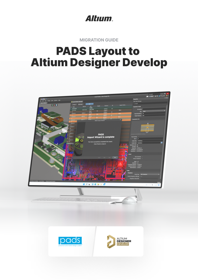
Migration Guide Making the Switch from PADS to Altium Designer Duplicate
14 min
Guide Books
Users of Competitor Tools
THE ALTIUM DESIGNER PHILOSOPHY At the core of Altium Designer
®
is one central theme - a unified approach to PCB
阅读文章
MENTOR PADSからALTIUM DESIGNERへの移行
1 min
Guide Books
Users of Competitor Tools
阅读文章
LEITFADEN ZUR ALTIUM VAULT IMPLEMENTIERUNG
1 min
Guide Books
阅读文章
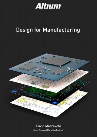
Design for Manufacturing Guidebook
123 min
Guide Books
This guidebook offers a comprehensive look at design for manufacturing, and how to ensure your PCB design will be manufacturable at high yield. We've included over 100 pages with detailed examples, a huge glossary, and much more.
阅读文章
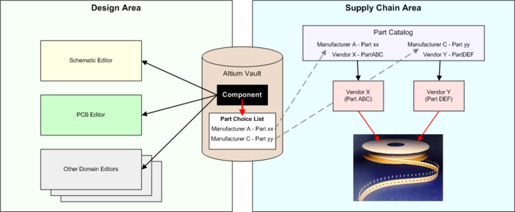
Component Management
1 min
Guide Books
阅读文章
Pagination
First page
« First
Previous page
‹‹
Page
12
Page
13
Page
14
Page
15
当前页面
16
Page
17
Next page
Next ›









 沪公网安备 31010502006411号