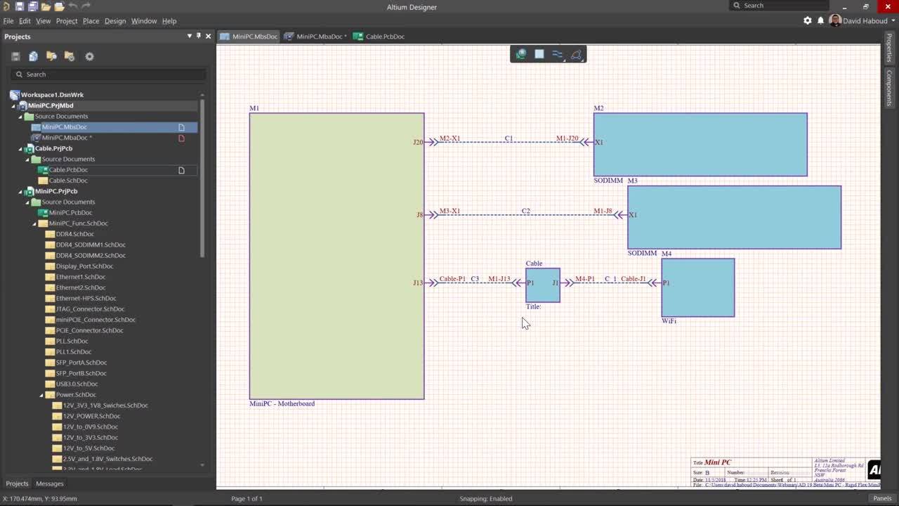
使用软硬结合设计和单板设计创建多板装配件。
Explore Altium Designer 24 technical documentation for Creating a Harness Wiring Component and related features.
Explore Altium Designer 24 technical documentation for Defining the Wiring Diagram and related features.
Explore Altium Designer 24 technical documentation for Creating the Layout Drawing and related features.
Explore Altium Designer 24 technical documentation for Creating a Manufacturing Drawing and related features.
Explore Altium Designer 24 technical documentation for Multi-board Schematic Preferences and related features.
Explore Altium Designer 24 technical documentation for Multi-board Assembly Preferences and related features.
Explore Altium Designer 24 technical documentation for Harness Design Preferences and related features.
This page looks at the PCB Editor's support for via stitching (used to tie together larger copper areas on different layers) and via shielding (used to help reduce crosstalk and electromagnetic interference in a route that is carrying an RF signal)
This page looks at the PCB Editor's support for embedded components - components that are manufactured as discrete entities and then placed on an inner layer of the circuit board during fabrication/assembly
Explore Altium Designer 24 technical documentation for Validating the Harness Design and related features.