


Work at Peak PCB Design Efficiency with Altium Designer


Are you unnecessarily repeating steps that are slowing your design workflow down? Many designers feel the pressure of continuous product deliveries and rapid design cycles, and design engineers need tools to maintain PCB design efficiency. The circuit design process doesn’t need to be repetitive or tedious when you use the right printed circuit design tools. Altium Designer includes powerful design and layout features alongside manufacturing tools and report generators, helping you stay efficient and complete designs on time.
ALTIUM DESIGNER
The best PCB design software for professional printed circuit designers.
Whenever you can reuse existing resources, you can save time and cost involved in creating new products. Many design teams reuse older designs, and sometimes these designs are decades old. These older designs may use outdated technology, but they still fit into standardized products, such as backplanes. If you have design tools that let you quickly create and copy project templates and other data, you can stay productive and reduce your total design time. Here’s how Altium Designer aids design reuse and ensures PCB design efficiency.
Challenges in Design Reuse and Data Management
The challenges involved in design reuse span from poor design tools to incoherent data management processes. Some design tools include the features needed to quickly reuse project data, but design data becomes unreadable if a precise file management system is not implemented. Similarly, some PCB design software isn’t built to allow design reuse; it doesn’t allow users to create PCB project templates, reusable circuit blocks, or multi-channel schematic diagram files for simple data reuse.
Altium Designer is Built for Design Reuse
Altium Designer is unique in that it supports project templates and reusable circuit blocks through its unified design environment. Storing older design data as a project layout template provides design reuse and allows access to all project files from a single location. In addition, the CAD features in Altium Designer help you create reusable design snippets, proprietary components, and schematic sheets for new projects. The unified design environment then links these elements together as you add them to your new projects.
- Working with snippets in your PCB layout helps you quickly replicate circuit blocks across your layout and reduces your design time.
See how PCB layout snippets help you quickly layout portions of your circuit board.
- Other design platforms can create unsolvable errors when you want to reuse old design data. The unified data model and file structure in Altium Designer helps prevent these errors and makes them easy to solve.
Learn more about solving component library errors during design reuse.
- Keeping your design data organized and properly tracked makes design reuse easy. Altium Designer helps you enforce this organization and keeps you productive during design reuse.
Learn more about managing your design data with your PCB design tools.

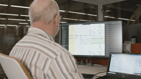
Daughterboard creation from PCB project templates in Altium Designer.
PCB Design Productivity with Layout Templates and Design Reuse
Today’s electronics engineers are under constant pressure to finish projects on increasingly shorter product schedules. Designs are always becoming more complex, and more complex designs are more difficult to modify once you need to create a variant. With all the complexities of PCB design, organizations continue to seek methods for improving productivity.
While “design reuse” has become an industry catch-phrase, design reuse is quite easy when you create and use project templates. Creating a project template is as simple as making a copy of an existing design, clearing out the application-specific components, and saving a copy as a blank project. Designers can then copy this design template as a new project and begin creating a variant for their designs.
How Printed Circuit Design Tools Aid Design Reuse
Design reuse helps designers stay productive, but it can be an unwieldy process when used with the wrong circuit board design software. Your design tools need to support reusable circuit blocks in your layout to help quickly place repeated sections in your PCB layout. When you use hierarchical multi-channel schematic design tools, you can link repeated circuit blocks together into complex systems. These design features are also present alongside schematic capture features in Altium Designer, which helps you stay productive.
- All circuit board designs start in the schematic. You can quickly reuse design data when you use hierarchical multi-channel design tools for creating schematic sheets.
Learn more about design reuse with multi-channel schematics aid design reuse.
- Once you start creating your PCB layout, you can place repeating circuitry with reusable blocks in your CAD tools. Altium Designer makes this easy with a powerful PCB editor.
Learn more about reusable circuit blocks in Altium Designer.
- Design reuse is intended to reduce your design time for common projects. The right printed circuit design tools and methodologies will help you remain productive.

Use Altium Designer to quickly create project variants for your projects.
Stay Productive with Unified Design Tools
Every project you create in Altium Designer will include a complete set of design documents that can be used to help you prepare for manufacturing and run important simulations. By placing everything in a rules-driven design interface, your design tools can work together from the same dataset to help you stay productive.
Creating a new project in Altium Designer involves the use of a Project Wizard. The Project Wizard allows you to select from default project examples, or you can create your own template from scratch. These template features help you stay highly productive throughout your design process. When combined with the hierarchical multi-channel schematic design features and modular circuit blocks in your PCB layout tools, you’ll design at top productivity with Altium Designer.
Altium Designer Offers the Only Unified Design Environment
When you use Altium Designer, you’ll have a complete package of printed circuit design tools to help you stay productive. Project templates help you get started quickly and reuse existing designs as new project variants. The complete set of CAD tools help you modify everything from trace layouts to ground plane placement in your circuit board. If you’re tired of working in separate design programs for design, manufacturing, and simulation, try using Altium Designer’s unified environment.
- By placing everything you need for circuit board design and analysis in a single program, Altium Designer helps you work with peak efficiency. You’ll have all the tools you need for professional circuit design and report generation.
- Altium Designer also includes a complete set of advanced design features for rigid-flex PCBs and multi-board systems. You can stay productive and use PCB project templates with these advanced designs.
Learn more about the advanced multi-board design features in Altium Designer.
- When you use Altium Designer through the Altium 365 platform, you can create a PCB data management system that helps you keep track of components, design files, and PCB project templates.
Learn more about managing your PCB design data in Altium 365.

The unified design environment in Altium Designer helps you stay productive with integrated circuit design features and PCB project example templates for design reuse.
By placing everything you need for printed circuit design in a single program, Altium Designer facilitates all aspects of design reuse and helps you stay productive. Editing a project template is as easy as creating a blank project, and your layout templates can be reused across any number of variants.
Altium Designer on Altium 365 delivers an unprecedented amount of integration to the electronics industry until now relegated to the world of software development, allowing designers to work from home and reach unprecedented levels of efficiency.
We have only scratched the surface of what is possible to do with Altium Designer on Altium 365. You can check the product page for a more in-depth feature description or one of the On-Demand Webinars.

关于作者
Related Technical Documentation
相关资源
目录
从设计到发布,全程无阻碍
- 让评审始终关联到正确的版本
- 减少交接中的混乱和返工
- 更早发现采购与发布风险
- 可独立工作,按需共享
开始使用
Thank you, you are now subscribed to updates.

 沪公网安备 31010502006411号