


Online Circuit Block Diagram Maker: Your Guide to Building PCBs with Altium Designer


Some PCB design software packages make you feel like you’ve been bamboozled. On one hand, you’re told that you’ll have access to tools that will let you move through the entire design process. Then all of a sudden, you can’t finish your design without purchasing critical features as add-ons. Only Altium Designer integrates all the best design tools in a single circuit diagram maker. You can get access to free versions that include critical design tools to help you move from design to production.
ALTIUM DESIGNER
The best PCB design software package for turning circuit diagrams into a finished device.
Designing a great PCB all starts with wiring your circuit diagram. Forget about using pen and paper; a great PCB design software package should include all the tools you need in a circuit diagram maker. Your schematic diagram should be able to quickly access your component information in order to accurately show how components are connected on your next device. Your schematic needs to be an accurate reflection of your finished device.
Moving successfully from your schematic to a complete layout takes tools that synchronize with each other. Other software packages claim to give you these capabilities in a single software package until you’re told you need to purchase a basic feature as an add-on. Once you capture your schematic on a new board as an initial layout, you shouldn’t have to pay extra just to automatically route and validate your device.
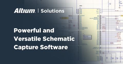
Building Your PCB Wiring Diagram Schematic
Your electronic schematic is like the blueprint for your new home. It shows the basics of how your circuit elements are connected to power, ground, and each other. Wires, resistors, a power supply, and copper will all be shown in their designed places so as to give your design visual life before production.
An electronic circuit doesn’t just come out of nowhere, though. Building a great PCB all starts with building a great schematic, and you’ll need a powerful wiring block diagram maker. Your editor should seamlessly interface with your component libraries and rules-checking features, ensuring that your PCB will work correctly.
Choosing the Schematic Editing Software
The best circuit diagram maker, online electrical schematic maker, and design editor synchronize directly with your PCB layout in a single software program. There is no reason your schematic editor should be separated from your layout editor, and your schematic should easily synchronize with your component management, simulation, and rules-checking tools. Your schematic editing software should also make it easy to synchronize changes between schematic and layout, ensuring that everyone on your team is capable of tracking any design changes.
- Every great device starts with an accurate and complete electronic schematic. Learn more about creating a great wiring schematic.
- Arranging components in your schematic can be like putting together a puzzle. Your schematic editor should make it easy to organize your components and route connections. Learn more about cleaning up a messy schematic.
- Routing is hugely simplified when you highlight nets directly in your schematic. This will help you save time routing components once you capture your schematic and build your layout. Learn more about highlighting signal nets in your schematic editor.

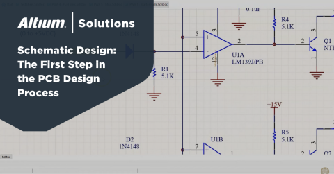
Schematic design in Altium Designer
Advanced Schematic Synchronization Features
Moving from schematic design to layout and beyond requires more advanced features that synchronize your PCB layout with your schematic. They should be able to organize your symbols and your drawing so that you can easily reference any design you’ve made.
Your schematic design and PCB layout tools should also synchronize with other features, such as your bill of materials generation tools, simulation and analysis tools, routing, and design rules checking. When all of these features work together, you’ll have the power to design advanced PCBs within a single design environment.
Advanced PCBs Need Advanced Circuit Diagram Makers
Designers working with advanced PCB applications need design tools that beautifully integrate changes in your layout, schematic, and component library updates. Moving from your circuit diagram to a layout requires a schematic capture tool and excellent routing tools. You can save a huge amount of time when your routing is automated. If you make changes to components in your layout, you need back annotation features that propagate your changes back to your schematic. This helps you keep your design organized.
- Your circuit schematic maker should quickly capture your design as a basic PCB layout. Learn more about best practices for schematic capture.
- Just like you can move from schematic to layout, you should be able to easily move in the other direction. Your design software should easily synchronize component or routing changes in your layout with your schematic. Learn more about back annotation to the schematic.
- Great PCB design software makes it easy to create project libraries directly from your schematic. Save time by reusing previous circuit diagrams instead of rebuilding from scratch. Learn more about creating project libraries from schematics in your circuit diagram maker.

Automated schematic back annotation
Building Circuits in Altium Designer’s Unified Environment
Let’s face it: a PCB design software program or wiring diagram maker usually doesn't have the best reputation. You’re only given a sample of the tools you need to actually build a functioning electronic device, and most of the tools are incomplete and inaccessible. Oftentimes, you are forced to use multiple tools from multiple sources just to get through the design process. You’re left hoping that your design data will move between programs without problems. Altium Designer's circuit diagram maker is your answer.
Altium Designer Has the Best Design Features Out of Any Circuit Diagram Maker
This is where Altium’s unified design environment has changed the game. As odd as it may sound, Altium actually wants you to have access to all the basic tools you need to take your PCB designs from start to finish, all in a single design package. Forget about using programs that tease you with high-end design features, you need a design program that actually gives you the capabilities to take you through the entire design and production process.
- Moving between your schematic and your layout requires routing that follows the pin mapping you’ve defined for your components. Routing in your schematic will easily translate into your layout, and automated routing makes it easy to finish your layout. Learn more about working with schematics in Altium Designer's circuit diagram maker.
- If you’re tired of routing everything by hand, you need a design package that can quickly route your traces according to your design rules. Get a sneak preview of the schematic editor enhancements in Altium Designer.
- Your unrouted PCB might look like a rat’s nest at first, but Altium Designer makes it easy to clean up your layout with powerful routing tools. Learn more about reusing features in Altium Designer's circuit diagram maker.
Working in a unified design environment means that your schematic and layout features work together to guide you through the entire design process. Altium Designer integrates your schematic design, layout, and component management tools in a single interface. This gives you the flexibility to design your circuits and layout for any application, and you’ll have the tools you need to move from design to production.
If you’re tired of other PCB design software companies or online electrical schematic drawing software teasing you with programs that aren’t even a complete package, then you need to try Altium Designer. The built-in CAD editing tools give you the power to build any circuit diagram, and your schematics easily synchronize with your layout. You’ll also have access to the best component management, rules-checking, and simulation tools, all within a single design environment.

关于作者
Related Technical Documentation
相关资源
目录
从设计到发布,全程无阻碍
- 让评审始终关联到正确的版本
- 减少交接中的混乱和返工
- 更早发现采购与发布风险
- 可独立工作,按需共享
开始使用
Thank you, you are now subscribed to updates.


 沪公网安备 31010502006411号