


Designing Physical Layer Security for Military PCBs in Altium Designer


PCBs for military systems are high performing beasts that must meet stringent design and performance standards. Military systems that store and process sensitive data require extra layers of security that goes beyond locking them in a secure enclosure. You’ll need to design your Printed Circuit Boards to be extremely resistant to EMI, route data so that it cannot be tapped passively, and include blacked-out chips to prevent attackers from accessing sensitive data. These measures for ensuring physical layer security for military Circuit Boards can be implemented when you use Altium Designer, the only fully integrated PCB design platform on the market.
ALTIUM DESIGNER®
A unified PCB design package with the best tools for designing military electronics systems.
Whether it’s a PCB for a computer peripheral, single board computer, or embedded system for data processing, military PCBs in mission critical systems must implement physical layer security measures. The right design software will help you design your military PCB to industrial standards and implement physical layer security protocols that are designed to prevent and detect circuit tampering.
Only Altium Designer integrates all of your design features on top of a single rules-driven design engine, giving you the adaptability you need to design any embedded system. You’ll have the power to design your board with the electrical performance required for mission critical applications, include components that help guarantee physical layer security, and tamper-proof communications capabilities. The integrated design, component management, and production planning environment in Altium Designer offers the tools required to implement physical layer security for military PCBs.
Physical Layer Security at the Board Level
Military systems that receive, process, and communicate data will do so using high-end commercially available components, and attackers can attempt circuit tampering directly at the component and trace level. There are a number of measures you can take that ensure these elements cannot be probed. Designing your Circuit Boards with these physical layer security measures is rather simple when you use the right design software.
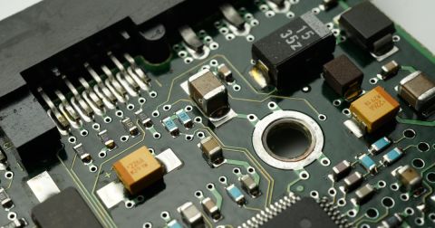
Sometimes, the best solutions are the least elegant. Vias are critical physical access points, and opting for the use of blind and buried vias will prevent vias with non-conductive fill decrease the number of locations that are vulnerable to physical probing. Using a thick solder mask to conceal and protect critical traces also prevents circuit tampering. Regarding components themselves, they should be blacked out so that attackers cannot directly identify manufacturers or model numbers. A component can also be encased in a non-conductive epoxy to physically prevent attackers from probing pins and capturing data.
Design Software for Board-level Security
Implementing physical layer security for military PCBs at the trace level might go so far as routing buried circuits in a multilayer board. Embedding as many components, traces, and vias as possible will limit opportunities for circuit tampering. Tamper detection is another measure that should be taken when possible. This involves designing packaging that will trip a fuse or switch if the enclosure is ever opened or damaged, cutting power to the board, and even alerting a base station.
All of these measures require carefully selecting your components so that you can ensure security and routing traces so that attackers are physically unable to access any elements that carry sensitive data. With the right design software, you can design any physical layer security measure into your board.
- Many of the physical layer security measures in IoT devices are implemented in PCBs for military systems. Learn more about physical layer security for PCBs.
- Burying traces and vias adds an extra physical layer security measure in your circuit board.
Learn more about working with blind and buried vias in Altium Designer.
- Burying traces using embedded microstrips or striplines is an excellent way to secure conductors from attackers. Learn more about the benefits of including striplines in your PCB.

Buried via design in Altium Designer
Securing Wireless Capabilities on the Physical Layer
Another critical aspect of physical layer security surrounds communications capabilities. Military systems with wireless capabilities should have enhanced shielding effectiveness against electromagnetic interference. This shielding should exceed radio frequency/electromagnetic interference standards on mission critical boards to prevent self-jamming. Communication between military systems often uses a custom wireless protocol in order to prevent unauthorized access and decoding of wireless data.
EMI Shielding Effectiveness and Security
Wireless data security must be implemented at the software/firmware level and at the component level. Preventing electromagnetic interference requires a number of smart design choices for any circuit board, but especially in boards with wireless capabilities. Just like the case of securing components, the brute force solution of using shielding cans can provide robust electromagnetic interference suppression in your PCB. Working with design software that integrates an extensive component library, mechanical tools, and electrical tools allows you to implement all of these measures in a single program.
- Embedding traces and vias is just one aspect of stackup design. When combined with the right routing practices, your stackup also helps suppress EMI from degrading signals in sensitive traces.
Learn more about designing your layer stackup with Rick Hartley.
- The right layout, routing, and component choices can help ensure signal integrity and immunity to EMI.
Learn more about best practices for ensuring signal integrity.
- Grounding and power integrity are critical aspects for ensuring signal integrity and providing EMI shielding. Learn more about designing and analyzing your power delivery network.

Designing a ground plane in a multilayer board provides robust EMI shielding
Design and Simulation in a Single Environment
With trace routing, via design, component selection, and packaging design being so important for physical layer security, you need design software that places all these tools into a single program. When these design tools integrate directly into your simulation features, you’ll have the power to design for physical security and electromagnetic interference immunity in a single program. Only Altium Designer places all these tools into a single environment.
Altium Designer: Unifying Your Design and Simulation Tools
The design and simulation features in Altium Designer are built on top of a rules-driven design engine, ensuring your tools communicate in the same data format and within the same program. Other programs separate design, simulation, production planning, and management features into different programs. No other design platform offers the same depth and breadth of functionality as Altium Designer.
- The unified environment in Altium Designer places all your important design tools and much more into a single program. Learn more about Altium Designer’s integrated PCB design environment.
- Given the demand for EMI shielding in physical layer security, your design software must include a comprehensive stackup materials library. Learn more about the stackup materials library in Altium Designer.
- Routing through interior layers with blind and buried vias is just one measure for implementing physical layer security in military PCBs. See how you can design blind and buried vias in Altium Designer.
Although attacks on consumer, industrial, and even military software systems seem to turn into major news stories on a weekly basis, rest assured that attackers are also interested in compromising physical devices. Working with the right PCB design package with an integrated feature set gives you the tools to implement physical layer security for military PCBs and help prevent tampering.
Altium wants you to be successful and will be there with resources when you need them. You’ll have access to design tutorials from industry experts, the AltiumLive forum, webinars and podcasts, and an extensive knowledge base. While other PCB design software companies leave you to work alone, Altium provides the knowledge and resources you need to reach success.
The rules-driven design engine in Altium Designer unifies your design features under one roof and is the new industry standard in PCB design. If you want to work with the best software on the market, then make the switch to Altium Designer.

关于作者
Related Technical Documentation
相关资源
目录
从设计到发布,全程无阻碍
- 让评审始终关联到正确的版本
- 减少交接中的混乱和返工
- 更早发现采购与发布风险
- 可独立工作,按需共享
开始使用
Thank you, you are now subscribed to updates.


 沪公网安备 31010502006411号