


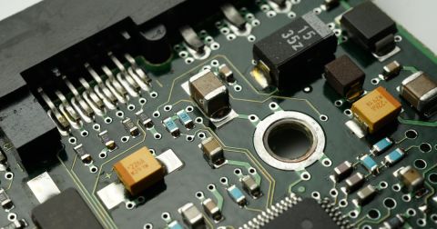


Engineering a Layer Stack Up for High Speed Design


Most of your board's simpler EMI/EMC problems, signal integrity problems, and power integrity problems can be solved or reduced with the right layer stackup. In high-speed PCB design and in RF PCB design, the layer stackup is the first place to start engineering the board to ensure it will operate within the intended operational parameters. But like any engineered component, a high-speed layer stackup must balance many functional goals, as well as aspects like cost and manufacturability.
To help designers develop a process for engineering a layer stackup that can support high-speed signals in a PCB, we've compiled a set of resources that explains some of the most important aspects of high-speed PCB layers stacks. There are many material systems and layer arrangements that will support high-speed signaling, but defining performance objectives and design constraints can help convergence to the best PCB layer stackup for a particular design.
A High-Speed Stackup Engineering Process
There are a few simple design goals involved in engineering a stackup:
- Determine layer counts
- Determine which types of materials are needed
- Determine Dk values based on layer thickness
- Make sure your fabrication house stocks your materials and can process your stackup
These points concern the design side of a high-speed PCB, but there is also manufacturability to consider, as described below.
How Many Layers Are Needed?
This is probably the most common question from new designers who realize they have to work with some high-speed interfaces in their board. Getting an estimate of the number of layers starts from a few important perspectives, such as the number of rows/columns in your BGA and the number of interleaved ground layers required in the PCB.
Although high-speed PCBs are sometimes associated with higher layer count PCBs, there are many high-speed systems that are designed on 4-layer PCBs. The 4-layer PCB and 6-layer PCB are probably the most common for digital systems because they are least expensive to scale to high volume in terms of fabrication costs. Therefore, you will see these in consumer electronics that have a lot of features included. 6-layer PCBs can also support HDI buildup and routing into some very dense BGA components with ball pitch less than 0.5 mm, which would be seen in consumer mobile or wearable devices.
High Speed Layer Stackup Materials
In products operating with high-bandwidth digital signals (>5 GHz), the materials used in the board should probably be the first point to begin building a design. In these systems, the main factor driving material selection is the dielectric and copper loss, the thickness required to hit a layer count goal, or both.
Most designers will probably default to a PTFE-based material with fiberglass reinforcement, but there are other resin laminate systems that can provide comparable or lower losses in long channels. It's important to examine whether the low losses found in these more expensive material systems are really needed in your particular PCB. In smaller boards, ultra-low loss may not be needed unless signal bandwidths reach far into the mmWave range, but larger boards with longer routes will be insertion loss dominated and will need lower losses.
As you enter the high layer count regime in boards that require large amounts of power to function properly, you will find that the typical sheet of FR4 laminate does not do enough to ensure power integrity. This can happen despite the use of a plane pair consisting of adjacent power and ground layers. To make up for the resulting power instability, there are embedded capacitance materials that can be used in paired power/ground plane layers. These materials can have higher Dk value, which causes the power/ground plane pair layer to act like a large capacitor with very low lead inductance. In addition, these materials can be intentionally lossy in order to dampen power transients .
Types of Stackup Materials
The above section concerns high-speed materials from their electrical and layer thickness perspectives. ECM materials and advanced resin-fiberglass composite laminates can also be very thin. However, there are other types of materials and material properties that might be very important for your particular board. For example, you may need to ask these questions:
- How much outgassing can your system tolerate?
- Will the board be thermally cycled? How much z-axis expansion will this produce?
- Are my targeted materials available or processable with my required type of copper foil?
- Will the operating temperature of the board exceed a certain Tg value?
- If I use an unreinforced material (e.g., PTFE), will there be excessive misregistration?
The answers to these questions will limit your material options to a certain subset of compatible high-speed materials.
Cost and Manufacturability
After determining the basic constraints and requirements on your PCB stackup, as well as some material options where necessary, it's important to get an idea of cost and manufacturability for the PCB stackup. Not all prototype manufacturers can or will use certain materials you request, and they will vary in terms of cost based on the level of service you need. As your layer count scales much higher, the board costs will also go up due to the need for more assembly steps to build the stackup, and the etching/processing requirements when feature sizes scale smaller.

High-speed PCBs can be difficult to design without the right CAD platform, so make sure you use the complete set of product design features in Altium Designer®. The CAD features in Altium Designer enable all aspects of systems and product design, ranging from packaging and PCB layout, and up to harness and cable design. When you’ve finished your design, and you want to release files to your manufacturer, the Altium 365™ platform makes it easy to collaborate and share your projects.
We have only scratched the surface of what’s possible with Altium Designer on Altium 365. Start your free trial of Altium Designer + Altium 365 today.

关于作者
Related Technical Documentation
相关资源
目录
从设计到发布,全程无阻碍
- 让评审始终关联到正确的版本
- 减少交接中的混乱和返工
- 更早发现采购与发布风险
- 可独立工作,按需共享
开始使用
Thank you, you are now subscribed to updates.


 沪公网安备 31010502006411号