


Guide to PCB Edge Plating in RF Design

At a Glance
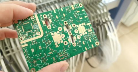
RF designs sometimes use PCB edge plating to contain electromagnetic fields and ruggedize a PCBA.


Some designs make use of edge plating around the exterior of a PCB, where the sidewalls of the PCB substrate are plated up with copper. The copper plating used in RF PCBs is placed for multiple reasons, such as providing a ground connection to a shielded enclosure or containing electromagnetic fields. If you determine you need to include edge plating, how should you specify this in your PCB layout and manufacturing data?
This article will give a short overview of how to apply edge plating in your PCB layout, as well as how edge plating will look in your fabrication deliverables. Make sure you follow these design rules for successful application of edge plating in your PCB layout.
Design Rules for Edge Plating
DFM Rules
The first important set of design rules are the DFM rules for edge plating. Edge plating is typically applied in two ways. The first method applies the edge plating as a separate copper structure that is disconnected from other copper pour on the PCB. This can be done when applying a guard ring around the edge of a PCB, which is typically done when applying a chassis ground.
The image below shows typical attachment distances and clearances that need to be applied between copper pour in the interior of the board and the edge plating. Note that the pour defining the edge plating extends over the board edge by about 0.5 mm; this can be reflected in the PCB layout with a design rule (see below).

In the above case, the edge plating would be applied by assigning it to its own net. If you give the ring its own net name, you can create a net-specific clearance rule for the board edge that will allow the pour to extend over the board outline. You can also use this rule to set the required clearance between the edge plating and the non-connected copper.
The other option is to completely wrap a polygon pour layer around the entire edge of the PCB and back to the other surface layer. In this case, the same clearance on the top layer would still apply, just like we had in the other arrangement. The above would typically not be used with a chassis ground, instead it would only apply to a system GND.

In the PCB Layout
To apply edge plating in the PCB layout, the plating needs to be defined using polygon pour. The polygon pour can then be run up to the edge of the PCB. The typical practice in ECAD software is to further extend the copper pour over the edge of the PCB. The copper plating extension distance over the edge can be small, typically by the 20 mil/0.5 mm distance shown in the above images.
To do this in Altium Designer, you can set a Board Outline Clearance rule. If you set the clearance to a negative value, it will allow the polygon to pour outside of the board edge.
If you have any edge-mounted connectors in the PCB layout, be careful after applying the polygon extension over the board edge. The polygon can extend around the pad and will create the potential for a short circuit; this might be expected at the center mount for an SMA edge connector. To prevent this problem, use a polygon cutout region around the pad to prevent edge plating in that region.

The process above is shown for edge plating, but it also applies to board cutouts in the interior region of the PCB. Once the plating region is defined and the design rules are set, remove the solder mask along the edge so that the area can be accessed for plating. This will also ensure the plating can make contact with any external metal as required, such as in a shielded enclosure.
Fabrication Data
Once you export your fabrication files, the copper will appear over the edge of the board outline layer. Typically a fabricator would send you an email asking questions and ensuring there was no error in your design files. To ensure you can get into fabrication quickly without getting these design questions, you should make sure your build requirements are properly communicated.

To do this, include a note in your fabrication drawing. You should include something like the following:
- PLATING TO BE ALONG BOARD EDGE. FINISHED THICKNESS OF EDGE PLATING TO BE X MILS +/- Y MILS.
Finally, if you need to complete a quote form for your order, make sure edge plating is included on the quote form so that there is no ambiguity as to your design intent.
Anytime you need to place unique copper structures in an RF PCB layout, including edge plating, use the complete set of PCB design and production tools in Altium Designer®. Once you’ve finished your PCB layout and you’re ready to share your manufacturing deliverables, you can easily share data and release files to your team with the Altium 365™ platform.
We have only scratched the surface of what’s possible with Altium Designer on Altium 365. Start your free trial of Altium Designer + Altium 365 today.

关于作者
Related Technical Documentation
相关资源
从设计到发布,全程无阻碍
- 让评审始终关联到正确的版本
- 减少交接中的混乱和返工
- 更早发现采购与发布风险
- 可独立工作,按需共享
开始使用
Thank you, you are now subscribed to updates.


 沪公网安备 31010502006411号