


.
独立的 Altium 365 Gerber 对比查看器提供免费访问,可通过网络浏览器以图形方式查看 Gerber 制作文件之间的差异。这为在发布迭代之间或将电路板生产数据发送给制造厂之前检查设计的制造输出提供了快速、简便的解决方案。 作为 Altium 开发和提供的免费服务,Gerber Compare 查看器无需下载、安装软件或注册即可提供全部功能。支持多种常见的 Gerber 文件包,包括 Altium Designer 和其他 ECAD 应用程序生成的 Gerber 输出文件,甚至包括硬件供应商提供的 Gerber 数据。 ►可通过www.altium.com/gerber-compare或在线 Altium 365 查看器中的 按钮访问在线Gerber 比较工具--更多信息请参见独立 Altium 365 查看器页面。 您可以上传两个 Gerber 数据集…
父页面: 工作区项目 Altium 365 工作区项目视图提供了设计数据比较功能,允许您比较不同项目发布和/或提交之间发生的数据变化。这些功能对于在将产品数据发送到制造方面之前进行最终检查特别有价值,它们允许您确切地确定您的 Gerber、原理图、PCB 和 BOM 数据在发布/提交事件之间发生了什么变化。 Gerber 比较 在将制造板数据发送给制造商之前进行最后检查总是一件好事。Gerber比较功能就是为此而设,能够快速检查以确保您的设计项目发布迭代之间在制造输出上没有差异。它提供了纯粹的图形化、逐层比较,通过使用边界框和数字来突出显示变化区域。 访问Gerber比较功能 可以通过以下方式访问Gerber比较功能: 点击项目详细管理页面的发布视图中与特定项目发布相关联的按钮。选择Gerber 到选项,并选择与之对比的其他发布的制造数据,或者对比一个已上传的文件集。 ``` ```…
当 BOM.CoDesign 处于 Released 状态时——请用“Public Feature Moves to Released”代码片段的源代码更新下方的蓝色框。 当在 Advanced Settings dialog 中启用 BOM.CoDesign 选项时,即可使用 BOM CoDesign 功能。 BOM CoDesign 功能促进 ECAD 与采购(Procurement)领域之间的协同 BOM 设计。该功能使设计人员与采购专家能够基于通过 BOM Portal 创建的 Related BOM 快照进行交互。BOM CoDesign 让你可以轻松查看设计的实时 WIP BOM 与所选采购 BOM 之间差异的摘要,并对其进行详细分析。对于检测到的每一处差异,你都可以完全控制是否将相应更改(如适用)应用到 ActiveBOM 文档中。 可从 Altium 365…
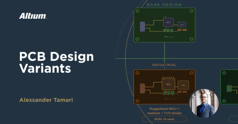
When a product needs to be designed and produced as a number of variations of that product, say where each has different options or capabilities, the ability to implement Design Variants avoids the need to create a unique version of the design for each variation. In practice, a Design Variant uses the same base design, but the PCB assembly is loaded with the set of components specified by the…
A large variety of outputs can be generated for and from a PCB design, and each output type has its own settings. The best way to manage this multitude of outputs in Altium Designer is to use an Output Job file, or 'OutJob' as it is more commonly known. An OutJob is simply a pre-configured set of outputs. Each output is configured with its own settings and its own output format, for example…
The final phase of the board design cycle is to generate the output files needed to fabricate, assemble and test the printed circuit board. To do this, you need to generate a variety of output files, in a variety of formats. The ultimate objective is to fabricate and assemble the board. As the designer you have the choice of individually configuring and generating the outputs via the schematic…
Print-based output for your PCB project in Altium Designer is available through creating a output job configuration file (*.OutJob). When you create a job output there is a range of manufacturing documentation available for output including common two-dimensional PCB printouts, such as a composite drawings and schematic drawings. 2D print output is configured in the PCB Printout Properties dialog…
Parent page: More about Outputs In Altium Designer, the ability to take a snapshot of your PCB as a 3D printout provides a quick and easy way to share the look of the finished product with others, prior to physical production of the board. However, there's always something lacking when it comes to a single 3D print. You inevitably want to tilt the board, rotate it, or flip it between component…
Altium Designer users have long enjoyed the ability to interactively view PCB designs in fully rendered 3D, which provides a unique insight into the real structure of the board design, its components and associated mechanical parts. There are significant advantages in being able to bring this 3D capability to those outside the immediate design team, such as fabrication and assembly houses, and…
PCB层是由曝光于光线下的胶片制成的。孔径是光线照射到胶片上的物理开口。CAM数据包括孔径定义(大小和形状),以及关于通过孔径闪光的位置,以及通过保持光束开启状态在位置之间移动来在胶片上绘制线条的指令。通过在胶片上闪光不同的孔径,将创建不同的焊盘大小;通过通过更大或更小的孔径拖动光束穿过胶片,将在胶片上绘制更厚或更薄的轨迹。 随着技术的发展,物理孔径可能完全退出PCB制造过程。即使现在,许多现代激光绘图仪也超越了对物理透镜孔径的需求,通过光栅操作在胶片上模拟相应的形状。 到目前为止,这些进步并没有改变我们谈论CAM图像的方式。每个CAM文件都需要一个孔径列表,无论这些图像是否真的会通过物理孔径转移到胶片上。你创建的每一个新的CAM文档都会包含一个空的孔径表。当你导入带有嵌入式孔径的CAM数据时,比如RS-274-X Gerber格式或ODB++数据,这个表会自动填充…
Learn More