


Use a PCB Gerber Viewer to Inspect Your Fab Files in Altium 365

At a Glance
A PCB Gerber viewer can help you inspect your board as you prepare for manufacturing. Use the features in Altium 365 to compare and share your Gerber files.


Your Gerber PCB software communicates your design to fabricators in a universal file format. Your Gerbers will show the arrangement of copper, solder mask, solder paste, silkscreen, and drill hits as needed to fabricate the PCB. Manufacturers can quickly put revisions through a design review with PCB Gerber viewer and compare features as you work through revisions on a project. Altium 365 makes this feature easy to access and easy to use through a cloud-based platform.
Your PCB design tools must be comprehensive, covering everything from schematic design and editing to layout and manufacturing preparation. Gerber files are among the most critical manufacturing files used in PCB fabrication processes. As part of a circuit board design review, manufacturers can use a Gerber viewer to inspect each layer of a printed circuit board and prepare stencils for each layer.
Most EDA tools can take your circuit board layout and generate detailed Gerber files, including layer stack information and standard image input formats for copper layers, the solder mask, and silkscreen. Altium Designer includes a file generator for Gerber X and X2 formats and Gerber viewer features in the CAMtastic tool, but comparing Gerber files has long required an external application. With Altium 365, a manufacturer can open Gerber files from two project revisions and compare them side-by-side. Designers can create their project releases with Gerber files in Altium Designer, and they can quickly push data to their manufacturer.
Use the Best Design Features With a PCB Gerber Viewer
A PCB Gerber viewer is a convenient utility for viewing each of the layers in a PCB. Gerber files show the arrangement of copper, solder mask, silkscreen, drill hits, and paste mask required to fabricate a finished circuit board. You can inspect your Gerber files with Altium Designer’s CAM processor tools regardless of which ECAD application you used to create your PCB.
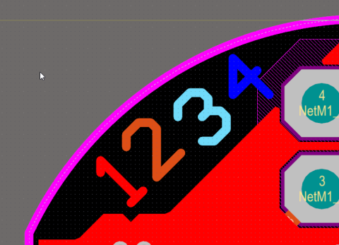
Once a design is submitted for fabrication, a PCB Gerber viewer will inspect the manufacturing files and call out design changes. Each layer within the stack may be inspected for pad and via attributes, layer pairs, mechanical layers, drill guides, and keep-out layers. In addition, features on the respective PCB layer, or layers, maybe highlighted for cross-probe with the schematic. All design files, including overlays, solder masks, drill files, and silkscreen, facilitate smooth communication with fabrication houses.
Altium Designer Includes More Than a PCB Gerber Viewer
Altium Designer gives you much more than just PCB Gerber viewer features. The industry’s best design tools are available in Altium Designer’s unified interface alongside a complete set of manufacturing and supply chain utilities. Cross-probing is available when making design corrections to ensure high manufacturing yield, so items highlighted within the PCB will be highlighted within the schematic. Everything needed to design, inspect, and manufacture a PCB and confirm design intent is available in Altium Designer.
- Gerber files have become the de facto standard for manufacturing files. The best PCB Gerber viewer will handle Gerber RS274X and X2 formats, as well as ODB++, IPC-2581, and IPC-D-356 formats.
Learn more about Gerber files and other manufacturing file formats.
- A PCB Gerber viewer helps designers and fabricators spot common DFM errors that occur in many PCB designs.
Learn more about some common DFM problems in circuit board layouts.
- Altium Designer includes an integrated tool to generate and view Gerber files alongside its other industry-standard design features. No other design application offers this many features to help you manufacture successfully.
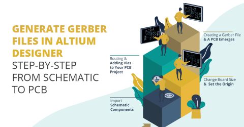
See how you can quickly generate Gerber files in Altium Designer.

Altium Designer offers complete control over all features in a PCB layout and helps designers stay productive.
Get Through Design Reviews with a Gerber Viewer
Before your board can be put into manufacturing, it must pass a thorough design review to ensure high yield and compliance with standards. Your PCB layout also needs to be checked against your design rules to ensure no errors in the layout that might reduce yield. What’s the fastest way to get your board into fabrication and ensure compliance with critical industry standards?
Altium 365 and Altium Designer work together to provide the answer. Altium Designer’s complete set of PCB layout and manufacturing tools is ideal for preparing your new design for fabrication and assembly. The sharing tools in Altium 365 give your fabricator direct access to your manufacturing files. This makes it easy for everyone to stay productive as a new design is prepared for manufacturing.
Inspect All File Formats in Altium Designer and Altium 365 Gerber Viewer
Altium 365 is the only online Gerber viewer platform that integrates directly with Altium Designer. View the latest Gerber X2 formats, IPC-2581 formats, and the Gerber RS-274X standards. Incorporating complete manufacturing details such as layer stack definitions, materials, netlists, test points, and NC drill files unleashes your manufacturing teams to build the PCB correctly on the first pass.
- Some standard PCB manufacturing defects can be spotted in Gerber files during a design review. Your manufacturer will use your Gerber files to inspect all aspects of your board and prepare stencils for fabrication.
Learn more about the role of Geber files in PCB design reviews before fabrication.
- Placing your PCB Gerber viewer features online in Altium 365 helps your team stay productive as you work with a manufacturer to pass a design review.
See how your team can stay productive with online collaboration features in Altium 365.
- When you use Altium 365, you can access an online PCB Gerber viewer for your Altium Designer circuit board projects without using an external application.
See how Altium 365 is changing the PCB industry and enabling remote collaboration.

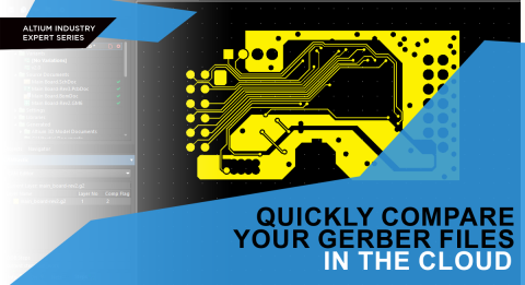
Once you’ve packaged your projects and shared them with your manufacturer through Altium 365, your manufacturer can compare old and new Gerber files for a project using the Gerber compare feature. The PCB Gerber viewer in Altium Designer accepts Gerber RS-274X and X2, along with ODB++, IPC-2581, and IPC-D-356. This means the viewer is backward compatible, allowing evaluation of any collection of artwork for your PCBs.
Altium 365 takes this a step further and includes Gerber compare features in an online interface. This is the fastest way to quickly find and inspect differences in Gerber files as you work through a design review to put your boards into production. The PCB Gerber viewer and compare features in Altium 365 support all file formats in your web browser. Project releases can also be opened in Altium Designer and inspected using the standard PCB Gerber Viewer features.
Stay Productive With a Complete Set of PCB Design Features
Altium Designer’s complete set of printed circuit board design and manufacturing features help you quickly generate documentation for fabrication and assembly. Still, it also includes the best circuit board design features. The rules-driven design tools in Altium Designer unify all your important circuit board design features in a single application, including PCB Gerber viewer, and compare features. Best of all, projects stored on the Altium 365 platform can be instantly opened into Altium Designer, helping design teams stay productive.
- Altium Designer’s rules-driven design engine unifies all your basic design, layout, sourcing, and manufacturing preparation features in a single application and helps you stay productive.
Learn more about the unified environment in Altium Designer.
- When you need to share your circuit board designs with your manufacturer, you can instantly publish your design and production data through the Altium 365 platform.
Learn more about sharing your design and production data with Altium 365.
- Use Altium Concord Pro to organize your projects when you need to manage the on-premises design and component data. No other application provides this type of enterprise-level solution that integrates with Altium Designer.

Easily create high-quality circuit designs, PCB layouts, and manufacturing documentation in Altium Designer and Altium 365.
When you need to quickly generate and publish Gerber files for your design and send your manufacturing documentation to your manufacturer, use Altium Designer and the Altium 365 platform. No other design application provides a complete set of design, sharing, and PCB Gerber viewer features in a single application.
Altium Designer on Altium 365 delivers unprecedented integration to the electronics industry until now relegated to the world of software development, allowing designers to work from home and reach unprecedented levels of efficiency. You won't find a better Gerber PCB software anywhere else.
We have only scratched the surface of what is possible to do with Altium Designer on Altium 365. You can check the product page for a more in-depth feature description or one of the On-Demand Webinars.

关于作者
Related Technical Documentation
相关资源
目录
从设计到发布,全程无阻碍
- 让评审始终关联到正确的版本
- 减少交接中的混乱和返工
- 更早发现采购与发布风险
- 可独立工作,按需共享
开始使用
Thank you, you are now subscribed to updates.
 沪公网安备 31010502006411号