


Follow Mixed Signal PCB Design Guidelines With the Best CAD Tools


Mixed-signal PCB design guidelines require satisfying basic digital and analog design rules and preventing signal interference. Guidelines can be difficult to lay out without the right PCB design tools, and component placement is just as important as routing and stack-up design. A good mixed-signal PCB design integrates the functionalities of digital and analog circuits. With the best PCB design software in Altium Designer, you can take your mixed-signal electronics from concept to finished product in a single application. You’ll have everything you need for schematics, PCB layout, manufacturing, and much more in a single program.
ALTIUM DESIGNER
A unified PCB design application with circuit design features, a powerful PCB editor, and simulation features for professional mixed-signal PCB designers.
High-speed digital PCBs are challenging enough to design, but what about a mixed-signal layout? Many modern systems contain elements that operate with both digital and analog signaling, and these systems must be designed to ensure signal integrity in both domains. These systems may operate in multiple frequency bands, including low-speed and high-speed digital signaling, and require these sections to interface with each other.
These objectives in mixed-signal layout for PCB design can be difficult to achieve when you don’t have the best design software. Altium Designer has the layout and signals integrity tools you need to ensure your mixed-signal PCB design does not experience interference and obeys important design standards. With a powerful set of layout and routing tools, you can follow the standard mixed-signal layout for PCB design guidelines outlined in this article. Keep reading to learn more.
Important Mixed-Signal Design Guidelines
There are many objectives in mixed-signal design, and these are intended to help suppress interference between different types of signals. Important aspects of high-speed/high-frequency PCB design need to be considered, such as controlled impedance routing and adhering to channel operating margin. The major design objectives in mixed-signal systems include:
- Maintaining isolation between digital and analog sections of a PCB
- Separating digital and analog components into their own circuit blocks
- Creating dedicated routing channels between analog and digital sections
- Preventing crosstalk and interference between these sections
- Establishing a consistent ground system throughout the board
- Ensure impedance control on critical analog and digital interconnects
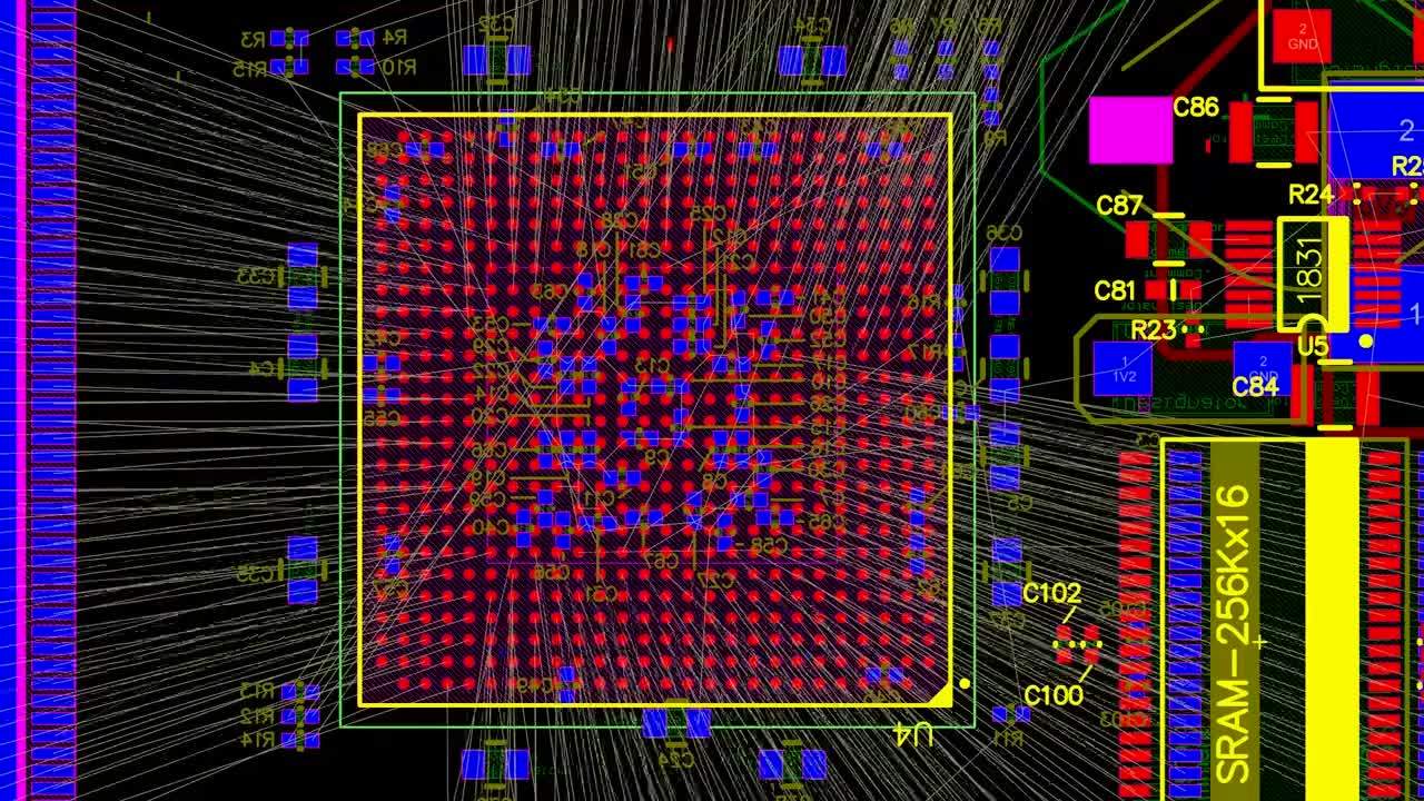
Perhaps the most important guideline in complex mixed-signal layout for PCB designs is to separate the system into different sections to help ensure isolation between critical signals. This helps prevent crosstalk between signals and components operating at different frequencies. The key here is to use the best routing features that help track an accurate return path through the system to ensure crosstalk does not occur between different board sections.

Partitioning in a mixed-signal layout helps provide isolation and prevent interference.
Ensure Accurate Mixed-Signal PCB Design with the Best Routing Features
Altium Designer’s PCB layout tools and routing features are designed to help you satisfy the above objectives in any circuit board. The need for controlled impedance and consistent ground plane design is satisfied with the integrated Layer Stack Manager in Altium Designer. Once copper plane layers are selected and impedance profiles are created, layout and routing in different regions of the board can begin with interactive routing features and accurate CAD tools.
- Your PCB layer stack-up design will determine the allowed return paths for your mixed signal design circuit board design. Be sure to track your return paths throughout your PCB layout to prevent mixed-signal interference.
Learn more about mixed-signal layout return paths in your PCB stack-up.
- The best circuit board layout features in Altium Designer will help you work at GHz frequencies in mixed-signal electronic systems.
Learn more about the design and layout for GHz band radio designs in Altium Designer.
- When it’s time to verify your mixed-signal design, Altium Designer makes it easy to export your design data into Ansys with its EDB Exporter extension. You can verify mixed-signal interference, spot excessive emissions, and much more with powerful field solvers.
Learn more about interfacing your design with Ansys SIwave for mixed-signal EMI analysis.

Create the best mixed-signal layout PCB designs in Altium Designer.
Integrated Schematic Capture to Start Your PCB Layout
Every mixed-signal design will start as schematics, where components are selected and circuits are designed. Mixed-signal layout boards face many of the same supply chain and organization problems that any other design will face, and designers need tools to help them stay organized as they create their schematics. Instead of using basic schematic design software, use Altium Designer’s integrated hierarchical multi-channel editor with an integrated schematic capture tool. You’ll stay organized, find the components you need, and easily transition to a PCB layout.
A Hierarchical Multi-channel Approach to Mixed-Signal PCB Design
Mixed-signal layout for PCB design is much easier when you use the best schematic editor to start your design and engineer your circuits. The hierarchical schematic editor tools in Altium Designer help you stay organized, and multi-channel schematics allow you to easily reuse circuits from one of your schematic sheets. This simplifies system-level design at the schematic level and helps organize your design before it’s transferred to a blank PCB layout.
When you’re ready to capture your schematics and begin your PCB layout, the integrated schematic capture feature in Altium Designer instantly imports your components into a blank PCB layout. You won’t need to use separate programs for schematic design, mixed-signal simulations, or schematic capture, everything you need can be found in Altium Designer.
- Working with hierarchical multi-channel schematic design tools helps speed up your circuit design and analysis processes through efficient design reuse.
See how hierarchical design helps you stay organized and work efficiently.
- Altium Designer’s schematic editor integrates a powerful SPICE package for running mixed-signal circuit simulations directly from your schematics.
Learn more about running SPICE simulations in Altium Designer.
- Navigating supply chain disruptions in mixed-signal circuit design is easy when your design software helps you find in-stock, in-production components for your PCB.
Learn more about supply chain visibility in Altium Designer’s sourcing features.

Find components, create your schematic designs, and use schematic capture to create your PCB layout in Altium Designer.
Getting Your Mixed-Signal Layout to Manufacturing
Your design process doesn’t end once you’ve finished your layout, and you’ll need to prepare your design for manufacturing at full scale. To help you make the transition to production, Altium Designer includes a complete set of manufacturing preparation tools that automate file generation in standard formats. After using integrated and 3rd party simulation features, mixed-signal circuit designers can quickly prepare their boards for high-volume manufacturing. You can take advantage of the following manufacturing features in Altium Designer:
- Generate Gerber files in the latest file formats (RS-274-X and X2)
- Fabrication and assembly drawing generation with the Draftsman utility
- Prepare a bill of materials and automatically import supply chain data
- NC drill file, pick-and-place file, and netlist generation
Altium Designer’s major advantage over other PCB design software applications is in its integration within a single environment. You no longer need separate applications for design, layout, schematic capture, and simulation, everything you need for mixed-signal layout for PCB design is in one software platform. Altium Designer helps you stay productive and design cutting-edge technology with the industry's most powerful PCB design application for product development.
Experience Rules-Driven Design in Altium Designer
The rules-driven design engine in Altium Designer gives you everything needed to design a complete system from concept to finished product. When you need to create a high-frequency analog system, high-speed digital circuit board, or mixed-signal PCB design, the rules-driven design environment in Altium Designer helps you stay productive and produce new products at scale.
- Altium Designer is a complete circuit board design application for any digital, analog, or mixed-signal system. Access everything you need for high-quality PCB designs in Altium Designer.
Learn more about the integrated design environment in Altium Designer.
- Mixed-signal designs need impedance control to ensure accurate interconnect design and routing. Altium Designer’s integrated field solver from Simberian gives mixed-signal layout and RF designers everything they need to accurately interconnect design calculations.
Learn more about the integrated field solver from Simberian in Altium Designer.
- When you’re ready to share your printed circuit board mixed-signal design with other designers or your PCB manufacturer, Altium 365 lets you instantly share your design and production data through Altium Designer or on the web.
Learn more about sharing your PCB project data with Altium 365.

Design high-quality mixed-signal PCB layouts in Altium Designer.
Stop using separate programs for circuit design, PCB layout, and manufacturing. Instead, take control over all aspects of your mixed-signal layout with the complete set of PCB design tools in Altium Designer. Only Altium helps you stay at the cutting edge of technology while helping you collaborate and stay productive.
Altium Designer on Altium 365 delivers an unprecedented amount of integration to the electronics industry until now relegated to the world of software development, allowing designers to work from home and reach unprecedented levels of efficiency.
We have only scratched the surface of what is possible to do with Altium Designer on Altium 365. You can check the product page for a more in-depth feature description or one of the On-Demand Webinars.

关于作者
Related Technical Documentation
相关资源
目录
从设计到发布,全程无阻碍
- 让评审始终关联到正确的版本
- 减少交接中的混乱和返工
- 更早发现采购与发布风险
- 可独立工作,按需共享
开始使用
Thank you, you are now subscribed to updates.


 沪公网安备 31010502006411号