


How to Make Your PCB Layout AOI and X-Ray Friendly

At a Glance
Designing for AOI and X-ray inspection boosts PCB yield and reliability. Learn layout tips that reduce defects, speed assembly, and cut costly surprises.


When we talk about design for manufacturability, it’s easy to get caught up in building the board itself. But there's another critical piece to the puzzle that deserves just as much attention: designing for inspection. Good inspection practice can be the difference between a board that performs reliably and one that ends up causing headaches after it leaves the factory floor.
Why Inspection Should Be on Your Radar
Inspection is about more than just spotting defects. It's about making sure the final product lives up to your design's potential. With all the complexity packed into today’s PCBs, relying on end-of-line testing alone just doesn’t cut it anymore. Automated Optical Inspection (AOI) and X-ray systems are your first line of defense, catching issues before they turn into costly field failures.
Boards that are designed with inspection in mind help build trust, trust that what you’ve designed is exactly what gets shipped. Plus, catching problems early means higher yields, lower costs, and fewer project delays.
AOI and X-Ray: Two Tools, Different Strengths
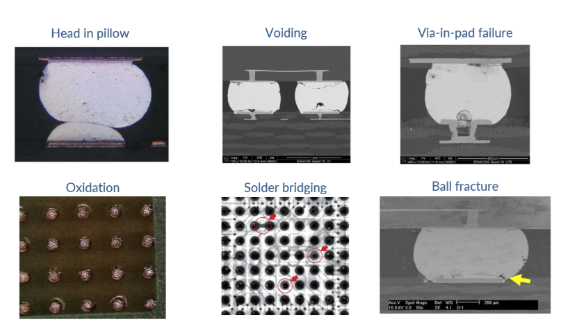
AOI uses high-resolution cameras and specific lighting setups to spot surface issues: missing components, lifted leads, tombstoning, solder bridges, you name it. It is fast, efficient, and great for catching problems early.
X-ray inspection, on the other hand, peeks inside the board to check what is hidden beneath components like BGAs and QFNs. It reveals voids in solder joints, misalignments, and hidden cracks, things that optical systems can't touch.
Each method has its own strengths and limitations and knowing what they can’t see is just as important as knowing what they can.
Design for Smooth, Accurate Inspection
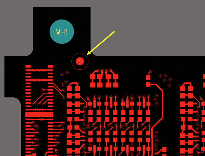
Let’s start with the basics: clear markings. AOI relies on fiducials and silkscreen markings to locate and inspect parts. Skimping here can throw off the entire process. Always include global fiducials, at least three per side, and add local ones around tricky components like BGAs. And do not hide your reference designators; if assembly covers them up, they're useless.
Component spacing is another simple but crucial factor. Tight layouts might save board space, but they can make inspection a nightmare. Leave enough room for the AOI cameras to "see" all the parts clearly. Also, try to avoid putting tall parts next to very short ones, it creates shadows that can trick the system.
Then there’s orientation. Try to align polarized parts consistently across the board. Diodes, capacitors, and ICs should all face the same way where possible. It makes AOI programming easier, and if a person has to step in, it’s immediately obvious when something’s wrong.
If you’re panelizing your design, give inspection a helping hand there too. Add fiducials on both the panel and the individual boards. Watch your breakaway tabs, make sure they don’t block critical areas or create obstacles for the inspection heads.
Now, onto BGAs and QFNs. This type of component is where X-ray shines, but only if you design for it. Keep pad sizes consistent and watch your solder paste volumes. If you overdo it, you’ll end up with voids that show up like big red flags under X-ray. When you’re laying out traces, think about the X-ray image, a clean, organized ground plane gives much sharper results than one that's cluttered with unnecessary vias.
False positives are another headache you can design your way out of. Make sure your footprints match real-world component sizes, avoid weird solder mask slivers, and carefully plan your solder paste apertures. The more predictable your board is, the less likely you are to waste time chasing down "problems" that aren’t really problems.
Get Your Manufacturer Involved Early
Want to really nail your design for inspection? Loop in your manufacturing team early. Share your component list, early stack-ups, draft Gerbers, whatever you have. Ask them to review and flag any areas that might cause trouble during inspection.
They’ve seen it all before, and they know what’s going to trip up AOI or muddy the waters for X-ray. A quick conversation now can save hours of troubleshooting later, not to mention saving you money and keeping your project timeline intact.
Also, don't underestimate how valuable these relationships are long-term. Partnering with your assembler and fabricator builds trust, shortens feedback loops, and helps everyone innovate faster. It’s a win for your current project, and every project after that.
Wrapping It Up
Designing for inspection isn’t just a box to check; it’s part of designing a reliable product. It’s about being proactive, not reactive. It’s about making sure your ideas aren’t just theoretically sound, but that they survive real-world manufacturing and deliver real-world reliability.
Small design tweaks, like better markings, smarter spacing, and cleaner layouts, can have a massive impact on your board’s inspectability. And that, in turn, means higher quality, better performance, and fewer headaches down the line.
Remember: a board that's easy to inspect is a board you can trust.
关于作者
Related Technical Documentation
相关资源
目录
从设计到发布,全程无阻碍
- 让评审始终关联到正确的版本
- 减少交接中的混乱和返工
- 更早发现采购与发布风险
- 可独立工作,按需共享
开始使用
Thank you, you are now subscribed to updates.


 沪公网安备 31010502006411号