


Practical Steps to Create Embedded Side-Emitting LEDs in a PCB

At a Glance
Embedded PCB cavities can be used along the edge of a PCB to provide side access to components, such as LEDs.


To meet the demands for product miniaturization, more people are turning to an embedded component. Embedded components (sometimes referred to as embedded passives when it's just a capacitor and resistor) are surface mount devices that can be added to inner layers of a multi-layer PCB, with cavities in the surrounding dielectric layers to allow them to be embedded inside the final PCB stack-up. Additionally, people are turning designs with a shift register, which share the same clocks and cascade throughout the design.
In this blog, Max Clemons (AE, Marketing) shows a novel approach for creating an embedded side-view LED that will display a shine from the very edges of the Printed Board he's working on, which are laminated into the layer stack.
Creating an Embedded Side-View LED
The Bluetooth Sentinel design, included with Altium Designer's installation, gives a good introduction to some of the new rigid-flex tools available. I was asked to modify this design to incorporate a different style of flexible region, but the repurposed board was left without room to place LEDs around its perimeter. Finding a way to add the LED strip is an interesting challenge, and gives the perfect opportunity to try out some of the new tools.
One of the cool new features added for Altium Designer is the ability to embed an electronic component within the board. This can be done for a number of reasons, including cutting down on space in very dense designs, and shortening return lengths in high speed applications. For the modified Bluetooth Sentinel design, an alternative was needed for the LEDs, and an embedded Side-View LED maintains the original functionality of the design tools, without having to modify it too much.
A thin package like the Everlight 48-213 SMD LED to the left was ideal for embedding, but really, the choice was only limited by the amount of vertical space available in the board. Creating this footprint was fairly straightforward, with only a couple minor additions to take advantage of the new features.
1. Start With a PCB Footprint
To get started, you can take an existing footprint and modify it to be embedded in a PCB cavity. First, make a copy of the component you want to embed before you modify the footprint.
If you don't already have the footprint and you can't find a footprint through online resources, you will need to make the footprint from scratch. Footprint information and package dimensions were both available in the datasheet. When creating a footprint, one of the fastest ways to achieve a good end result is to set an appropriate Reference Point and Grid spacing. From there, it’s simply a matter of placing Pads, 3D Bodies, and any additional Mechanical information required.

2. Define a 3D Body
Extruded bodies worked fine for most of the LED, the lens object being the lone exception. While the extruded bodies are surprisingly robust, and work well for polygonal shapes, the arced corners of the lens were more feasible to create externally and bring in as a STEP model.


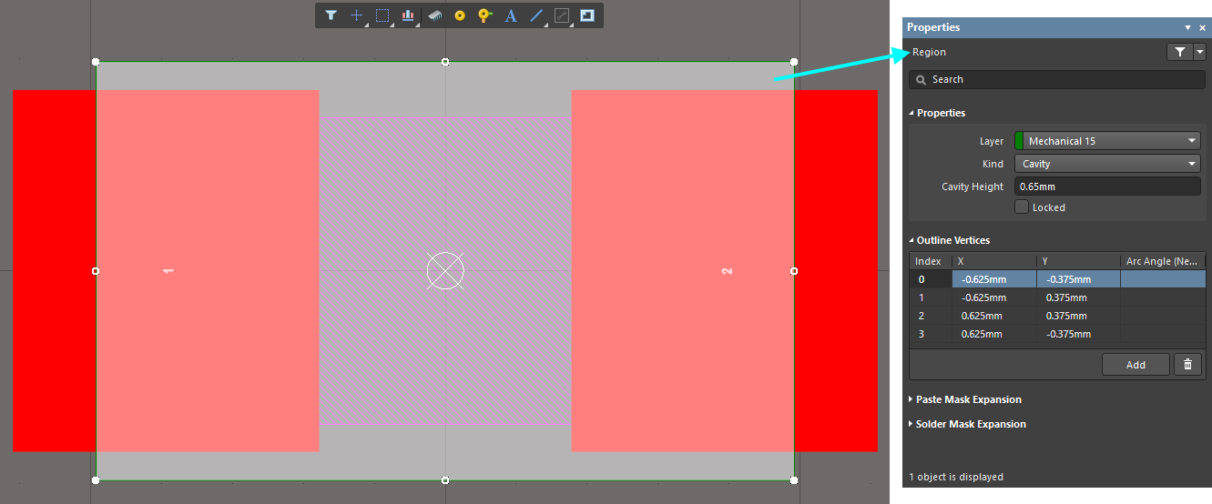
3. Cavities in a PCB Footprint
Preparing a component to be embedded starts from the footprint itself. A Cavity - simply a Solid Region configured as shown - must be placed in the panel. Its height, as defined from the Properties, should be just large enough to allow for the component body. The LED package was 0.3mm, so the Cavity was created with a height of 0.35mm. This, of course, will ultimately depend on your specific Layer Stack and overall design intent.
4. Place the Part to Place the Cavity
It’s important to note that Cavities can be placed within any footprint, whether or not it will ever be an embedded side-view LED. When the electronic component is placed on an inner layer, the Cavity will carve out a section of the core material, but on an outer layer, it won’t affect the design in any way. Placing one of the newly-created LEDs on an inner layer showed how cool this looks in action.

5. Embedded Cavities in the Stackup
Technically, a Cavity alters the Layer Stack in that particular area, and it’s crucial that this information is conveyed through fabrication notes. The Layer Stack Diagram that can be automatically generated and placed already takes this into account. In this design, there was no question where the Cavities were added, or what layers from the stackup were included in those areas.

6. The Assembly Process
Assembly must also be considered, since embedded components are placed before those on the outside of the board. It’s a good idea to create a separate pick and place report, as well as an extra assembly drawing printout, for any inner layers embedded with an electronic component.
I’ve included the footprint and completed design for reference, but this is certainly not the limit of how an embedded component can be used. Just an interesting way to solve this problem!
Download your copy of the project shown above:
- Bluetooth Sentinel Modified.zip
It's worth mentioning that the cavity can be a part of the electronic component even when it's not embedded - it just automatically does it's job when you move the component to inner layers.
Then it's also worth *mentioning* what fabrication and assembly outputs would be needed - the layer stack table showing cavity regions, as well as separate Pick and Place report for the embedded panel, since they are mounted in an earlier process step.

关于作者
Related Technical Documentation
相关资源
目录
从设计到发布,全程无阻碍
- 让评审始终关联到正确的版本
- 减少交接中的混乱和返工
- 更早发现采购与发布风险
- 可独立工作,按需共享
开始使用
Thank you, you are now subscribed to updates.


 沪公网安备 31010502006411号