


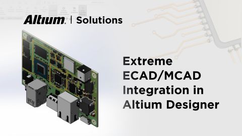


MOVE INTERFERENCE CHECKING TO ELECTRONIC DESIGN FOR A MORE EFFICIENT FLOW

At a Glance
The completed electronic design moves to mechanical designers for interference checking for electronic design. That iterative approach delays and can even cause missed deadlines.


Every electronic product consists of both mechanical and electrical assemblies. The two need to fit together — you don’t want electronic components interfering with the mechanical enclosure. Typically, the completed electronic design moves to mechanical designers for electrical interference checking. Any component interference problems are identified and then passed back to the electrical designer for necessary changes. It can take multiple iterations before the electronics properly fit within the enclosure. That iterative approach delays product completion. negatively affects schedules, and can even cause missed deadlines.
How do you shorten this timetable? You need a methodology that gives electrical designers the opportunity to verify interference before the design is handed off to mechanical designers. Using that methodology can reduce iterations, save time, and improve the overall accuracy of your schedule. Let’s look at how that methodology works.
MULTIPLE ECAD/MCAD ITERATIONS
Electrical designers commonly rely on mechanical designers to verify that the enclosure can accommodate the electronics without interference. This is because their electrical design tools may not be able to import a model of the mechanical enclosure. The tool also may not have the ability to import individual STEP models for placed components. So, the electrical designer must rely on the mechanical tool environment for further interference analysis.
Once the mechanical designer receives the electrical assembly, violations are then noted and relayed back to the electrical designer. If holes are misaligned or component parts collide, they must be corrected to the specifications provided by the mechanical designer. Once these changes are made on the ECAD side, the design is handed off to the mechanical designer. This flow goes on until no interference exists.
A BETTER APPROACH
The best way to reduce (or eliminate) iterations is for the electrical designer to verify clearance before it’s handed off to the mechanical team. STEP files can be imported for each component and then embedded as a component property. This STEP model can either be obtained from the manufacturer or manually created within the electrical design tool. Either way, it has the accurate physical dimensions of the component. Embedding dimensions moves toward the goal of interference checking taking place completely within ECAD.
STEP files are not limited to components. The mechanical housing itself can be imported as a STEP file from the mechanical designer. Once this data is obtained, you then import it into the ECAD tool and verify that the all of the components and connectors fit securely within the housing and mounting holes are where they belong. Any discrepancies can be quickly adjusted in the ECAD tool, eliminating the interference. Once verified, the final electrical assembly design moves to the mechanical team for any further testing. This methodology significantly reduces the number of iterations, saving time and money - and keeping the product on schedule.
INTERFERENCE CHECKING CAPABILITIES IN ALTIUM DESIGNER
Altium Designer supports both import and export of STEP models and files, allowing electrical inference checking within the electrical design. The component clearance rule verifies that all 3D bodies and models within the design adhere to the constraints you have defined.
The online design rule checking capability within Altium Designer notifies you of collisions and highlights the collisions location in green, identifying the violating primitives. There is also an identifier when a given STEP model or 3D body violates the specified clearance. The primitives that are being assessed are the STEP files of the components and the STEP file of the mechanical housing. The image below illustrates that the connectors do not correctly fit within the enclosure, so they are highlighted.

Figure 1 - Collision and clearance violations highlighted in green
The next figure shows the result of changes made to the connector positioning so that the electrical assembly fits securely within the housing.

Figure 2 - The absence of any highlighting means that the assembly now fits within the enclosure
CONCLUSION
Interference checking for electronic design is a necessary and critical part of the design process: quite simply, your product cannot be built if the electronic assembly does not fit in the enclosure. Passing a design back and forth between electrical and mechanical designers costs time and money. Checking clearances within the electrical design tool is a much better and more efficient option.
Moving electrical interference checking to an earlier point in the design flow requires an ECAD tool capable of importing component and enclosure STEP files and 3D rule checking. The unified environment of Altium Designer gives you more efficient avenues to complete the design process. The result is a quicker design time leading to on-time product release.
Useful Links:
Download the PDF to keep learning offline

关于作者
Related Technical Documentation
相关资源
目录
从设计到发布,全程无阻碍
- 让评审始终关联到正确的版本
- 减少交接中的混乱和返工
- 更早发现采购与发布风险
- 可独立工作,按需共享
开始使用
Thank you, you are now subscribed to updates.

 沪公网安备 31010502006411号